SNAS305J July 2005 – March 2016 ADC121S021
PRODUCTION DATA.
- 1 Features
- 2 Applications
- 3 Description
- 4 Revision History
- 5 Device Comparison Table
- 6 Pin Configuration and Functions
- 7 Specifications
- 8 Parameter Measurement Information
- 9 Detailed Description
- 10Applications Information
- 11Power Supply Recommendations
- 12Layout
- 13Device and Documentation Support
- 14Mechanical, Packaging, and Orderable Information
パッケージ・オプション
メカニカル・データ(パッケージ|ピン)
サーマルパッド・メカニカル・データ
発注情報
10 Applications Information
NOTE
Information in the following applications sections is not part of the TI component specification, and TI does not warrant its accuracy or completeness. TI’s customers are responsible for determining suitability of components for their purposes. Customers should validate and test their design implementation to confirm system functionality.
10.1 Application Information
The ADC121S021 is a successive-approximation analog-to-digital converter designed around a charge-redistribution digital-to-analog converter core. Simplified schematics of the ADC121S021 in both track and hold modes are shown in Figure 15 and Figure 16, respectively. In Figure 15, the device is in track mode: switch SW1 connects the sampling capacitor to the input, and SW2 balances the comparator inputs. The device is in this state until CS is brought low, at which point the device moves to the hold mode.
Figure 16 shows the device in hold mode: switch SW1 connects the sampling capacitor to ground, maintaining the sampled voltage, and switch SW2 unbalances the comparator. The control logic then instructs the charge-redistribution DAC to add or subtract fixed amounts of charge from the sampling capacitor until the comparator is balanced. When the comparator is balanced, the digital word supplied to the DAC is the digital representation of the analog input voltage. The device moves from hold mode to track mode on the 13th rising edge of SCLK.
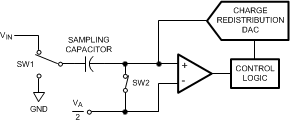 Figure 15. ADC121S021 in Track Mode
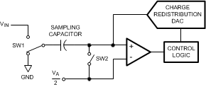 Figure 16. ADC121S021 in Hold Mode
10.1.1 Using the ADC121S021
The serial interface timing diagram for the ADC is shown in Figure 1. CS is chip select, which initiates conversions on the ADC and frames the serial data transfers. SCLK (serial clock) controls both the conversion process and the timing of serial data. SDATA is the serial data out pin, where a conversion result is found as a serial data stream.
Basic operation of the ADC begins with CS going low, which initiates a conversion process and data transfer. Subsequent rising and falling edges of SCLK is labeled with reference to the falling edge of CS; for example, the third falling edge of SCLK shall refer to the third falling edge of SCLK after CS goes low.
At the fall of CS, the SDATA pin comes out of TRI-STATE, and the converter moves from track mode to hold mode. The input signal is sampled and held for conversion on the falling edge of CS. The converter moves from hold mode to track mode on the 13th rising edge of SCLK (see Figure 1). It is at this point that the interval for the tACQ specification begins. At least 350 ns must pass between the 13th rising edge of SCLK and the next falling edge of CS. The SDATA pin is placed back into TRI-STATE after the 16th falling edge of SCLK, or at the rising edge of CS, whichever occurs first. After a conversion is completed, the quiet time (tQUIET) must be satisfied before bringing CS low again to begin another conversion.
Sixteen SCLK cycles are required to read a complete sample from the ADC. The sample bits (including leading zeroes) are clocked out on falling edges of SCLK, and are intended to be clocked in by a receiver on subsequent rising edges of SCLK. The ADC produces three leading zero bits on SDATA, followed by twelve data bits, most significant first.
If CS goes low before the rising edge of SCLK, an additional (fourth) zero bit may be captured by the next falling edge of SCLK.
10.1.1.1 Determining Throughput
Throughput depends on the frequency of SCLK and how much time is allowed to elapse between the end of one conversion and the start of another. At the maximum specified SCLK frequency, the maximum ensured throughput is obtained by using a 20 SCLK frame. As shown in Figure 1, the minimum allowed time between CS falling edges is determined by 1) 12.5 SCLKs for Hold mode, 2) the larger of two quantities: either the minimum required time for Track mode (tACQ) or 2.5 SCLKs to finish reading the result and 3) 0, 1/2 or 1 SCLK padding to ensure an even number of SCLK cycles so there is a falling SCLK edge when CS next falls. For example, at the fastest rate for this family of parts, SCLK is 20 MHz and 2.5 SCLKs are 125 ns, so the minimum time between CS falling edges is calculated in Equation 1:
Which corresponds to a maximum throughput of 1 MSPS. At the slowest rate for this family, SCLK is 1 MHz. Using a 20 cycle conversion frame as shown in Figure 1 yields a 20 μs time between CS falling edges for a throughput of 50 KSPS.
It is possible, however, to use fewer than 20 clock cycles provided the timing parameters are met. With a 1-MHz SCLK, there are 2500 ns in 2.5 SCLK cycles, which is greater than tACQ. After the last data bit has come out, the clock needs one full cycle to return to a falling edge. Thus the total time between falling edges of CS is
12.5 × 1 μs + 2.5 × 1 μs + 1 × 1 μs = 16 μs which is a throughput of 62.5 ksps.
10.1.2 ADC121S021 Transfer Function
The output format of the ADC is straight binary. Code transitions occur midway between successive integer LSB values. The LSB width for the ADC is VA / 4096. The ideal transfer characteristic is shown in Figure 17. The transition from an output code of 0000 0000 0000 to a code of 0000 0000 0001 is at 1/2 LSB, or a voltage of VA / 8192. Other code transitions occur at steps of one LSB.
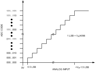 Figure 17. Ideal Transfer Characteristic
10.1.3 Analog Inputs
An equivalent circuit for the ADC's input is shown in Figure 18. Diodes D1 and D2 provide ESD protection for the analog inputs. The analog input must at no time go beyond (VA + 300 mV) or (GND – 300 mV), as these ESD diodes begins to conduct, which could result in erratic operation. For this reason, the ESD diodes must not be used to clamp the input signal.
The capacitor C1 in Figure 18 has a typical value of 4 pF, and is mainly the package pin capacitance. Resistor R1 is the ON-resistance of the track / hold switch, and is typically 500 Ω. Capacitor C2 is the ADC sampling capacitor and is typically 26 pF. The ADC delivers best performance when driven by a low-impedance source to eliminate distortion caused by the charging of the sampling capacitance. This is especially important when using the ADC to sample AC signals. Also important when sampling dynamic signals is an anti-aliasing filter.
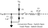 Figure 18. Equivalent Input Circuit
10.1.4 Digital Inputs And Outputs
The ADC digital inputs (SCLK and CS) are not limited by the same maximum ratings as the analog inputs. The digital input pins are instead limited to 5.25 V with respect to GND, regardless of VA, the supply voltage. This allows the ADC to be interfaced with a wide range of logic levels, independent of the supply voltage.
10.1.5 Power Management
The ADC takes time to power-up, either after first applying VA, or after returning to normal mode from shutdown mode. This corresponds to one dummy conversion for any SCLK frequency within the specifications in this document. After this first dummy conversion, the ADC performs conversions properly.
NOTE
The tQUIET time must still be included between the first dummy conversion and the second valid conversion.
When the VA supply is first applied, the ADC may power up in either of the two modes: normal or shutdown. As such, one dummy conversion must be performed after start-up, as described in the previous paragraph. The part may then be placed into either normal mode or the shutdown mode, as described in Normal Mode and Shutdown Mode.
When the ADC is operated continuously in normal mode, the maximum ensured throughput is fSCLK / 20 at the maximum specified fSCLK. Throughput may be traded for power consumption by running fSCLK at its maximum specified rate and performing fewer conversions per unit time, raising the ADC CS line after the 10th and before the 15th fall of SCLK of each conversion. A plot of typical power consumption versus throughput is shown in Typical Characteristics. To calculate the power consumption for a given throughput, multiply the fraction of time spent in the normal mode by the normal mode power consumption and add the fraction of time spent in shutdown mode multiplied by the shutdown mode power consumption.
NOTE
The curve of power consumption vs throughput is essentially linear. This is because the power consumption in the shutdown mode is so small that it can be ignored for all practical purposes.
10.2 Typical Application
A typical application of the ADC is shown in Figure 19. Power is provided in this example by the Texas Instruments LP2950 low-dropout voltage regulator, available in a variety of fixed and adjustable output voltages. The power supply pin is bypassed with a capacitor network located close to the ADC. Because the reference for the ADC is the supply voltage, any noise on the supply degrades the noise performance of the device. To keep noise off the supply, use a dedicated linear regulator for this device, or provide sufficient decoupling from other circuitry to keep noise off the ADC supply pin. Because of the ADC's low power requirements, it is also possible to use a precision reference as a power supply to maximize performance. The three-wire interface is shown connected to a microprocessor or DSP.
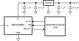 Figure 19. Typical Application Circuit
10.2.1 Design Requirements
A positive supply only data acquisition system capable of digitizing signals ranging from 0 V to 5 V and interfacing through SPI with an MCU whose supply is set at 3.3 V.
10.2.2 Detailed Design Procedure
The signal range requirement forces the design to use 5-V analog supply at VA, analog supply. This follows from the fact that VA is also a reference potential for the ADC.
Sampling is in fact a modulation process which may result in aliasing of the input signal if the input signal is not adequately band limited. The maximum sampling rate (fS) of the ADC121S021 when it is enabled is:
In order to avoid aliasing, the Nyquist criterion has to be met:
Therefore it is necessary to place an anti-aliasing filter at the input of the ADC. This filter may be a single-pole low-pass filter. The pole location need to satisfy Equation 4:
With fSCLK = 4 MHz, a good choice for the single pole filter is:
- R = 100 Ω
- C = nF
This reduces the input BWsignal = 250 kHz. The capacitor at the VIN input of the device provides not only the filtering of the input signal, but it also absorbs the charge kick-back from the ADC. The kick-back is the result of the internal switches opening at the end of the acquisition period.
Take care when the signal source is capable of producing voltages beyond VA. In such instances the internal ESD diodes may start conducting. The ESD diodes are not intended as input signal clamps. To provide the desired clamping action use Schottky diodes.
10.2.3 Application Curves
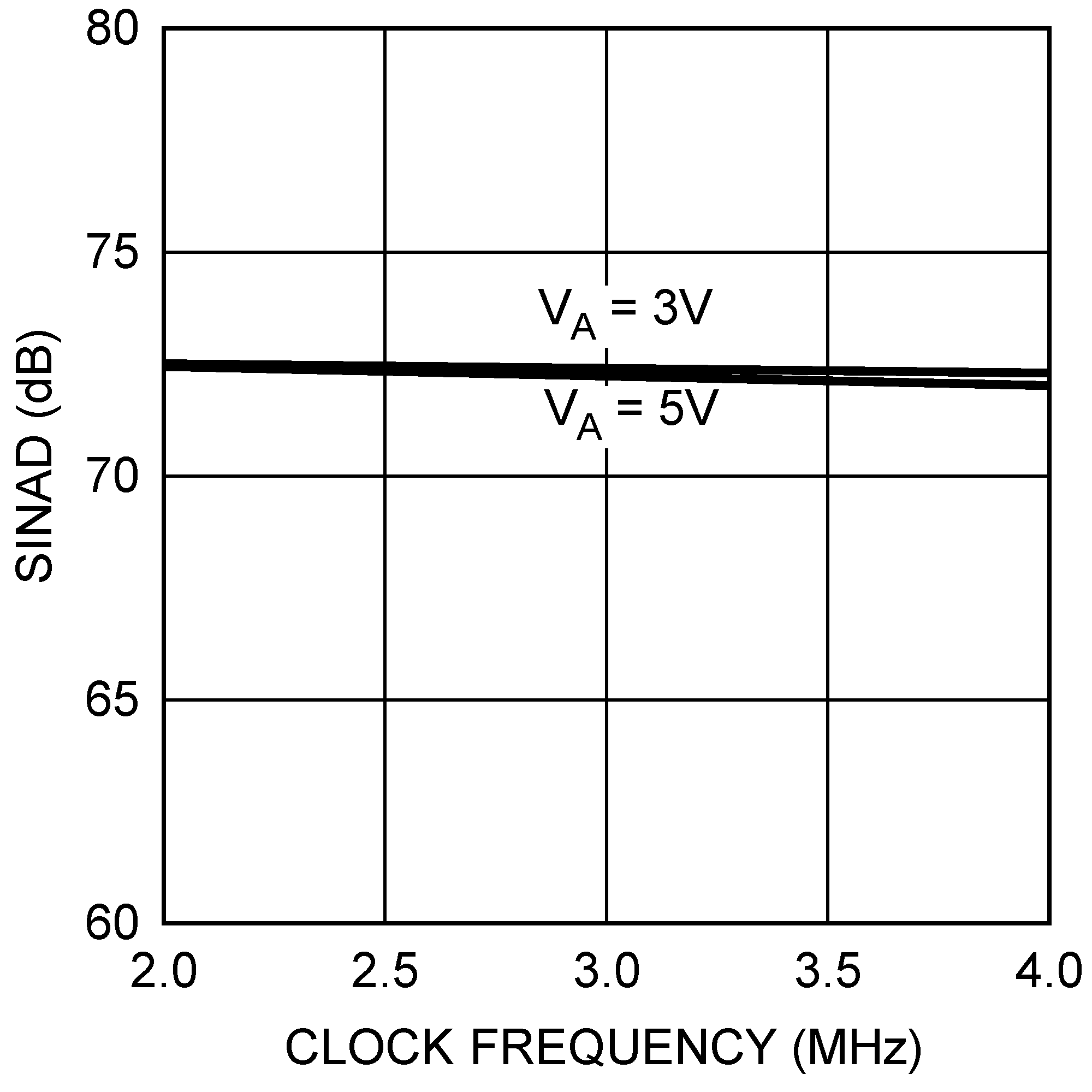
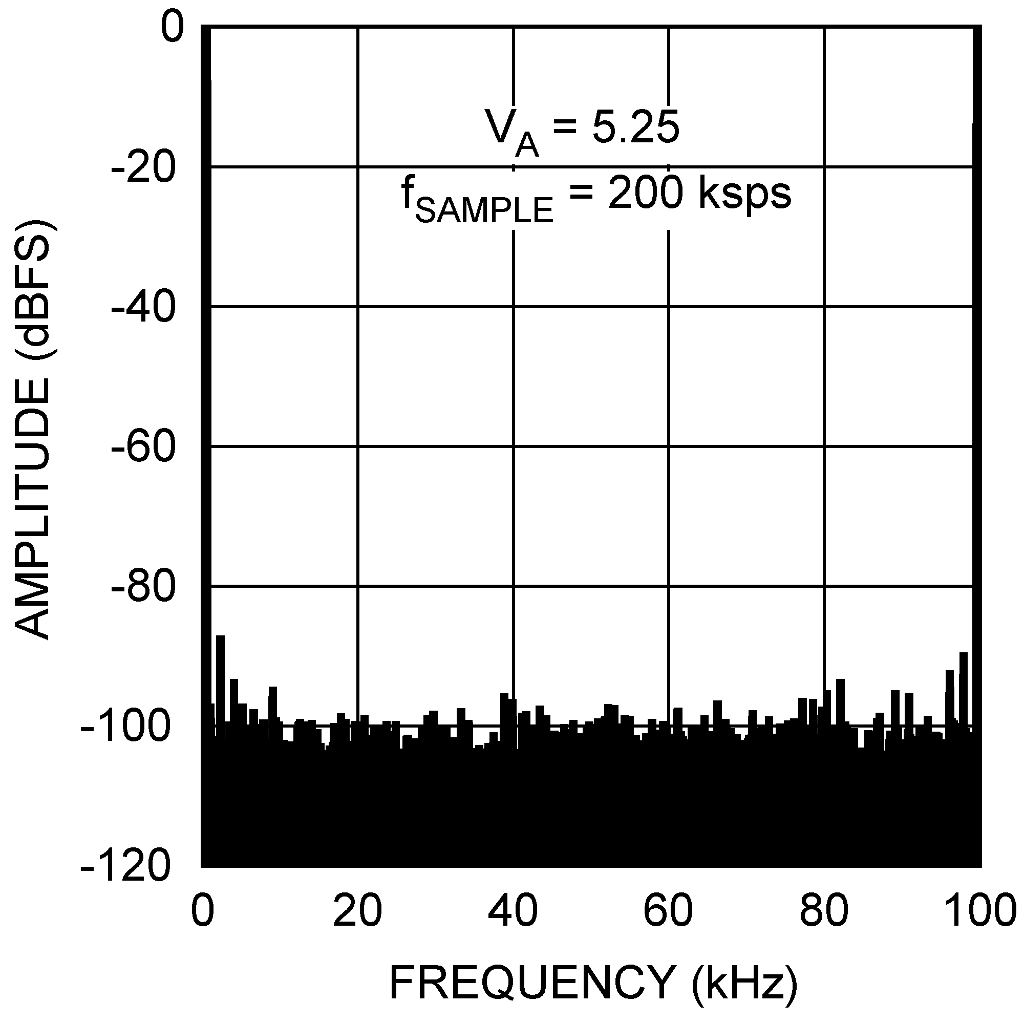
| VA = 5.25 V | fSCLK = 4 MHz |