JAJSEG6A January 2018 – April 2020 ADC12DJ2700
PRODUCTION DATA.
- 1 特長
- 2 アプリケーション
- 3 概要
- 4 改訂履歴
- 5 概要(続き)
- 6 Pin Configuration and Functions
-
7 Specifications
- 7.1 Absolute Maximum Ratings
- 7.2 ESD Ratings
- 7.3 Recommended Operating Conditions
- 7.4 Thermal Information
- 7.5 Electrical Characteristics: DC Specifications
- 7.6 Electrical Characteristics: Power Consumption
- 7.7 Electrical Characteristics: AC Specifications (Dual-Channel Mode)
- 7.8 Electrical Characteristics: AC Specifications (Single-Channel Mode)
- 7.9 Timing Requirements
- 7.10 Switching Characteristics
- 7.11 Typical Characteristics
-
8 Detailed Description
- 8.1 Overview
- 8.2 Functional Block Diagram
- 8.3
Feature Description
- 8.3.1 Device Comparison
- 8.3.2 Analog Inputs
- 8.3.3 ADC Core
- 8.3.4 Temperature Monitoring Diode
- 8.3.5 Timestamp
- 8.3.6 Clocking
- 8.3.7 Digital Down Converters (Dual-Channel Mode Only)
- 8.3.8 JESD204B Interface
- 8.3.9 Alarm Monitoring
- 8.4
Device Functional Modes
- 8.4.1 Dual-Channel Mode
- 8.4.2 Single-Channel Mode (DES Mode)
- 8.4.3 JESD204B Modes
- 8.4.4 Power-Down Modes
- 8.4.5 Test Modes
- 8.4.6 Calibration Modes and Trimming
- 8.4.7 Offset Calibration
- 8.4.8 Trimming
- 8.4.9 Offset Filtering
- 8.5 Programming
- 8.6
Register Maps
- 8.6.1 Memory Map
- 8.6.2
Register Descriptions
- 8.6.2.1
Standard SPI-3.0 (0x000 to 0x00F)
- Table 46. Standard SPI-3.0 Registers
- 8.6.2.1.1 Configuration A Register (address = 0x000) [reset = 0x30]
- 8.6.2.1.2 Device Configuration Register (address = 0x002) [reset = 0x00]
- 8.6.2.1.3 Chip Type Register (address = 0x003) [reset = 0x03]
- 8.6.2.1.4 Chip ID Register (address = 0x004 to 0x005) [reset = 0x0020]
- 8.6.2.1.5 Chip Version Register (address = 0x006) [reset = 0x01]
- 8.6.2.1.6 Vendor Identification Register (address = 0x00C to 0x00D) [reset = 0x0451]
- 8.6.2.2 User SPI Configuration (0x010 to 0x01F)
- 8.6.2.3
Miscellaneous Analog Registers (0x020 to 0x047)
- 8.6.2.3.1 Clock Control Register 0 (address = 0x029) [reset = 0x00]
- 8.6.2.3.2 Clock Control Register 1 (address = 0x02A) [reset = 0x00]
- 8.6.2.3.3 SYSREF Capture Position Register (address = 0x02C-0x02E) [reset = Undefined]
- 8.6.2.3.4 INA Full-Scale Range Adjust Register (address = 0x030-0x031) [reset = 0xA000]
- 8.6.2.3.5 INB Full-Scale Range Adjust Register (address = 0x032-0x033) [reset = 0xA000]
- 8.6.2.3.6 Internal Reference Bypass Register (address = 0x038) [reset = 0x00]
- 8.6.2.3.7 TMSTP± Control Register (address = 0x03B) [reset = 0x00]
- 8.6.2.4 Serializer Registers (0x048 to 0x05F)
- 8.6.2.5
Calibration Registers (0x060 to 0x0FF)
- 8.6.2.5.1 Input Mux Control Register (address = 0x060) [reset = 0x01]
- 8.6.2.5.2 Calibration Enable Register (address = 0x061) [reset = 0x01]
- 8.6.2.5.3 Calibration Configuration 0 Register (address = 0x062) [reset = 0x01]
- 8.6.2.5.4 Calibration Status Register (address = 0x06A) [reset = Undefined]
- 8.6.2.5.5 Calibration Pin Configuration Register (address = 0x06B) [reset = 0x00]
- 8.6.2.5.6 Calibration Software Trigger Register (address = 0x06C) [reset = 0x01]
- 8.6.2.5.7 Low-Power Background Calibration Register (address = 0x06E) [reset = 0x88]
- 8.6.2.5.8 Calibration Data Enable Register (address = 0x070) [reset = 0x00]
- 8.6.2.5.9 Calibration Data Register (address = 0x071) [reset = Undefined]
- 8.6.2.5.10 Channel A Gain Trim Register (address = 0x07A) [reset = Undefined]
- 8.6.2.5.11 Channel B Gain Trim Register (address = 0x07B) [reset = Undefined]
- 8.6.2.5.12 Band-Gap Reference Trim Register (address = 0x07C) [reset = Undefined]
- 8.6.2.5.13 VINA Input Resistor Trim Register (address = 0x07E) [reset = Undefined]
- 8.6.2.5.14 VINB Input Resistor Trim Register (address = 0x07F) [reset = Undefined]
- 8.6.2.5.15 Timing Adjust for A-ADC, Single-Channel Mode, Foreground Calibration Register (address = 0x080) [reset = Undefined]
- 8.6.2.5.16 Timing Adjust for B-ADC, Single-Channel Mode, Foreground Calibration Register (address = 0x081) [reset = Undefined]
- 8.6.2.5.17 Timing Adjust for A-ADC, Single-Channel Mode, Background Calibration Register (address = 0x082) [reset = Undefined]
- 8.6.2.5.18 Timing Adjust for C-ADC, Single-Channel Mode, Background Calibration Register (address = 0x083) [reset = Undefined]
- 8.6.2.5.19 Timing Adjust for C-ADC, Single-Channel Mode, Background Calibration Register (address = 0x084) [reset = Undefined]
- 8.6.2.5.20 Timing Adjust for B-ADC, Single-Channel Mode, Background Calibration Register (address = 0x085) [reset = Undefined]
- 8.6.2.5.21 Timing Adjust for A-ADC, Dual-Channel Mode Register (address = 0x086) [reset = Undefined]
- 8.6.2.5.22 Timing Adjust for C-ADC Acting for A-ADC, Dual-Channel Mode Register (address = 0x087) [reset = Undefined]
- 8.6.2.5.23 Timing Adjust for C-ADC Acting for B-ADC, Dual-Channel Mode Register (address = 0x088) [reset = Undefined]
- 8.6.2.5.24 Timing Adjust for B-ADC, Dual-Channel Mode Register (address = 0x089) [reset = Undefined]
- 8.6.2.5.25 Offset Adjustment for A-ADC and INA Register (address = 0x08A-0x08B) [reset = Undefined]
- 8.6.2.5.26 Offset Adjustment for A-ADC and INB Register (address = 0x08C-0x08D) [reset = Undefined]
- 8.6.2.5.27 Offset Adjustment for C-ADC and INA Register (address = 0x08E-0x08F) [reset = Undefined]
- 8.6.2.5.28 Offset Adjustment for C-ADC and INB Register (address = 0x090-0x091) [reset = Undefined]
- 8.6.2.5.29 Offset Adjustment for B-ADC and INA Register (address = 0x092-0x093) [reset = Undefined]
- 8.6.2.5.30 Offset Adjustment for B-ADC and INB Register (address = 0x094-0x095) [reset = Undefined]
- 8.6.2.5.31 Offset Filtering Control 0 Register (address = 0x097) [reset = 0x00]
- 8.6.2.5.32 Offset Filtering Control 1 Register (address = 0x098) [reset = 0x33]
- 8.6.2.6
ADC Bank Registers (0x100 to 0x15F)
- 8.6.2.6.1 Timing Adjustment for Bank 0 (0° Clock) Register (address = 0x102) [reset = Undefined]
- 8.6.2.6.2 Timing Adjustment for Bank 0 (–90° Clock) Register (address = 0x103) [reset = Undefined]
- 8.6.2.6.3 Timing Adjustment for Bank 1 (0° Clock) Register (address = 0x112) [reset = Undefined]
- 8.6.2.6.4 Timing Adjustment for Bank 1 (–90° Clock) Register (address = 0x113) [reset = Undefined]
- 8.6.2.6.5 Timing Adjustment for Bank 2 (0° Clock) Register (address = 0x122) [reset = Undefined]
- 8.6.2.6.6 Timing Adjustment for Bank 2 (–90° Clock) Register (address = 0x123) [reset = Undefined]
- 8.6.2.6.7 Timing Adjustment for Bank 3 (0° Clock) Register (address = 0x132) [reset = Undefined]
- 8.6.2.6.8 Timing Adjustment for Bank 3 (–90° Clock) Register (address = 0x133) [reset = Undefined]
- 8.6.2.6.9 Timing Adjustment for Bank 4 (0° Clock) Register (address = 0x142) [reset = Undefined]
- 8.6.2.6.10 Timing Adjustment for Bank 4 (–90° Clock) Register (address = 0x143) [reset = Undefined]
- 8.6.2.6.11 Timing Adjustment for Bank 5 (0° Clock) Register (address = 0x152) [reset = Undefined]
- 8.6.2.6.12 Timing Adjustment for Bank 5 (–90° Clock) Register (address = 0x153) [reset = Undefined]
- 8.6.2.7 LSB Control Registers (0x160 to 0x1FF)
- 8.6.2.8
JESD204B Registers (0x200 to 0x20F)
- 8.6.2.8.1 JESD204B Enable Register (address = 0x200) [reset = 0x01]
- 8.6.2.8.2 JESD204B Mode Register (address = 0x201) [reset = 0x02]
- 8.6.2.8.3 JESD204B K Parameter Register (address = 0x202) [reset = 0x1F]
- 8.6.2.8.4 JESD204B Manual SYNC Request Register (address = 0x203) [reset = 0x01]
- 8.6.2.8.5 JESD204B Control Register (address = 0x204) [reset = 0x02]
- 8.6.2.8.6 JESD204B Test Pattern Control Register (address = 0x205) [reset = 0x00]
- 8.6.2.8.7 JESD204B DID Parameter Register (address = 0x206) [reset = 0x00]
- 8.6.2.8.8 JESD204B Frame Character Register (address = 0x207) [reset = 0x00]
- 8.6.2.8.9 JESD204B, System Status Register (address = 0x208) [reset = Undefined]
- 8.6.2.8.10 JESD204B Channel Power-Down Register (address = 0x209) [reset = 0x00]
- 8.6.2.8.11 JESD204B Extra Lane Enable (Link A) Register (address = 0x20A) [reset = 0x00]
- 8.6.2.8.12 JESD204B Extra Lane Enable (Link B) Register (address = 0x20B) [reset = 0x00]
- 8.6.2.9
Digital Down Converter Registers (0x210-0x2AF)
- 8.6.2.9.1 DDC Configuration Register (address = 0x210) [reset = 0x00]
- 8.6.2.9.2 Overrange Threshold 0 Register (address = 0x211) [reset = 0xF2]
- 8.6.2.9.3 Overrange Threshold 1 Register (address = 0x212) [reset = 0xAB]
- 8.6.2.9.4 Overrange Configuration Register (address = 0x213) [reset = 0x07]
- 8.6.2.9.5 DDC Configuration Preset Mode Register (address = 0x214) [reset = 0x00]
- 8.6.2.9.6 DDC Configuration Preset Select Register (address = 0x215) [reset = 0x00]
- 8.6.2.9.7 Digital Channel Binding Register (address = 0x216) [reset = 0x02]
- 8.6.2.9.8 Rational NCO Reference Divisor Register (address = 0x217 to 0x218) [reset = 0x0000]
- 8.6.2.9.9 NCO Synchronization Register (address = 0x219) [reset = 0x02]
- 8.6.2.9.10 NCO Frequency (DDC A or DDC B and Preset x) Register (address = see ) [reset = see ]
- 8.6.2.9.11 NCO Phase (DDC A or DDC B and Preset x) Register (address = see ) [reset = see ]
- 8.6.2.10 Spin Identification Register (address = 0x297) [reset = Undefined]
- 8.6.2.1
Standard SPI-3.0 (0x000 to 0x00F)
- 8.6.3
SYSREF Calibration Registers (0x2B0 to 0x2BF)
- 8.6.3.1 SYSREF Calibration Enable Register (address = 0x2B0) [reset = 0x00]
- 8.6.3.2 SYSREF Calibration Configuration Register (address = 0x2B1) [reset = 0x05]
- 8.6.3.3 SYSREF Calibration Status Register (address = 0x2B2 to 0x2B4) [reset = Undefined]
- 8.6.3.4 DEVCLK Aperture Delay Adjustment Register (address = 0x2B5 to 0x2B7) [reset = 0x000000]
- 8.6.3.5 DEVCLK Timing Adjust Ramp Control Register (address = 0x2B8) [reset = 0x00]
- 8.6.4 Alarm Registers (0x2C0 to 0x2C2)
- 9 Application and Implementation
- 10Power Supply Recommendations
- 11Layout
- 12デバイスおよびドキュメントのサポート
- 13メカニカル、パッケージ、および注文情報
パッケージ・オプション
メカニカル・データ(パッケージ|ピン)
- ZEG|144
- AAV|144
サーマルパッド・メカニカル・データ
発注情報
8.3.7.2 Decimation Filters
The decimation filters are arranged to provide a programmable overall decimation of 2, 4, 8, or 16. All filter outputs have a resolution of 15 bits. The decimate-by-2 filter has a real output and the decimate-by-4, decimate-by-8, and decimate-by-16 filters have complex outputs. Table 11 lists the effective output sample rates, available signal bandwidths, output formats, and stop-band attenuation for each decimation mode. The available bandwidths of the complex output modes are twice that of equivalent real decimation modes because of the nature of the I/Q data and complex signaling. This higher bandwidth results in the decimate-by-2 real and decimate-by-4 complex modes having approximately the same useful output bandwidth.
Table 11. Output Sample Rates and Signal Bandwidths
| DECIMATION SETTING | ƒ(DEVCLK) | OUTPUT FORMAT | |||
|---|---|---|---|---|---|
| OUTPUT RATE (MSPS) | MAX ALIAS PROTECTED SIGNAL BANDWIDTH (MHz) | STOP-BAND ATTENUATION | PASS-BAND RIPPLE | ||
| No decimation | ƒ(DEVCLK) | ƒ(DEVCLK) / 2 | — | < ±0.001 dB | Real signal,
12-bit data |
| Decimate-by-2 | ƒ(DEVCLK) / 2 | 0.4 × ƒ(DEVCLK) / 2 | > 89 dB | < ±0.001 dB | Real signal,
15-bit data |
| Decimate-by-4
(D4_AP87 = 0) |
ƒ(DEVCLK) / 4 | 0.8 × ƒ(DEVCLK) / 4 | > 90 dB | < ±0.001 dB | Complex signal,
15-bit data |
| Decimate-by-4
(D4_AP87 = 1) |
ƒ(DEVCLK) / 4 | 0.875 × ƒ(DEVCLK) / 4 | > 66 dB | < ±0.005 dB | Complex signal,
15-bit data |
| Decimate-by-8 | ƒ(DEVCLK) / 8 | 0.8 × ƒ(DEVCLK) / 8 | > 90 dB | < ±0.001 dB | Complex signal,
15-bit data |
| Decimate-by-16 | ƒ(DEVCLK) / 16 | 0.8 × ƒ(DEVCLK) / 16 | > 90 dB | < ±0.001 dB | Complex signal,
15-bit data |
Figure 69 to Figure 80 provide the composite decimation filter responses. The pass-band section (black trace) shows the alias-protected region of the response. The transition band (red trace) shows the transition region of the response, or the regions that alias into the transition region, which is not alias protected and therefore desired signals must not be within this band. The aliasing band (blue trace) shows the attenuation applied to the bands that alias back into the pass band after decimation and are sufficiently low to prevent undesired signals from showing up in the pass band. Use analog input filtering for additional attenuation of the aliasing band or to prevent harmonics, interleaving spurs, or other undesired spurious signals from folding into the desired signal band before the decimation filter.
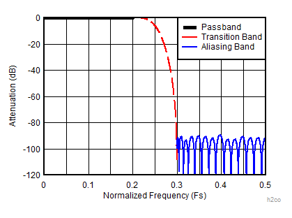
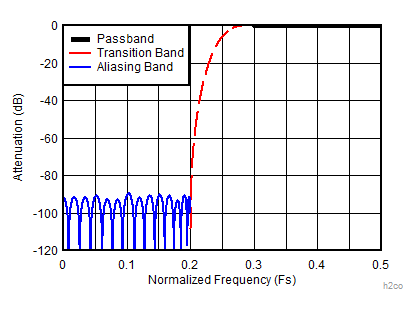
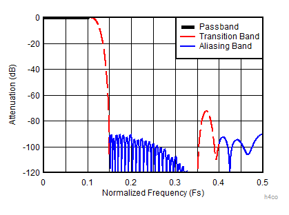
(D4_AP87 = 0)
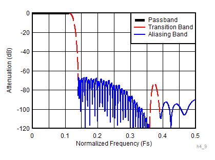
(D4_AP87 = 1)
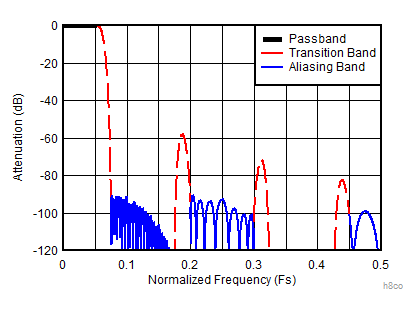
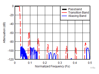
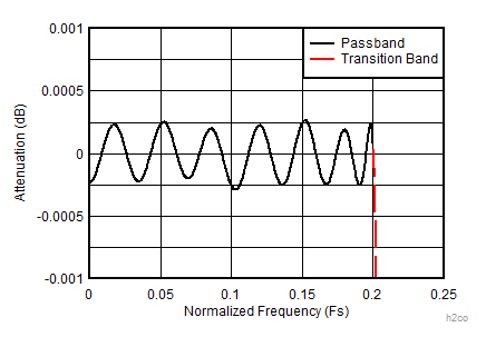
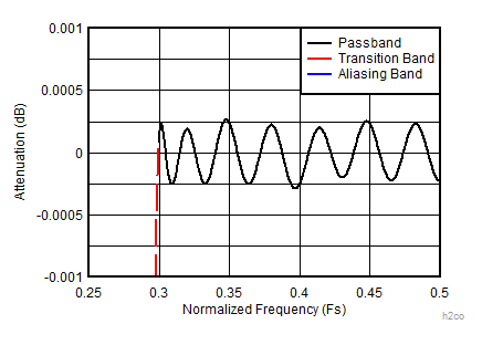
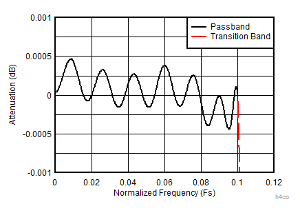
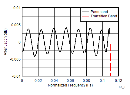
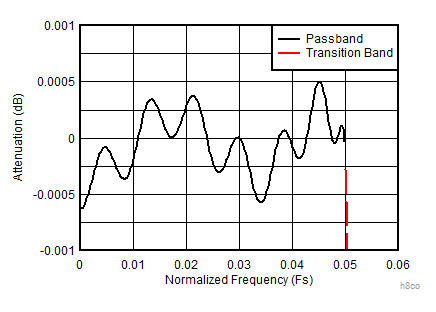
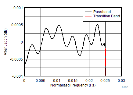
For maximum efficiency, a group of high-speed filter blocks are implemented with specific blocks used for each decimation setting to achieve the composite responses illustrated in Figure 69 to Figure 80. Table 12 describes the combination of filter blocks used for each decimation setting and Table 13 lists the coefficient details and decimation factor of each filter block. The coefficients are symmetric with the center tap indicated by bold text.
Table 12. Decimation Mode Filter Usage
| DECIMATION SETTING | FILTER BLOCKS USED |
|---|---|
| 2 | CS80 |
| 4 (D4_AP87 = 0) | CS45, CS80 |
| 4 (D4_AP87 = 1) | CS45, CS87 |
| 8 | CS20, CS40, CS80 |
| 16 | CS10, CS20, CS40, CS80 |
Table 13. Filter Coefficient Details
| FILTER COEFFICIENT SET (Decimation Factor of Filter) | |||||||||||
|---|---|---|---|---|---|---|---|---|---|---|---|
| CS10 (2) | CS20 (2) | CS40 (2) | CS45 (2) | CS80 (2) | CS87 (2) | ||||||
| –65 | –65 | 109 | 109 | –327 | –327 | 56 | 56 | –37 | –37 | –15 | –15 |
| 0 | 0 | 0 | 0 | 0 | 0 | 0 | 0 | 0 | 0 | 0 | 0 |
| 577 | 577 | –837 | –837 | 2231 | 2231 | –401 | –401 | 118 | 118 | 23 | 23 |
| 1024 | 0 | 0 | 0 | 0 | 0 | 0 | 0 | 0 | 0 | 0 | |
| 4824 | 4824 | –8881 | –8881 | 1596 | 1596 | –291 | –291 | –40 | –40 | ||
| 8192 | 0 | 0 | 0 | 0 | 0 | 0 | 0 | 0 | |||
| 39742 | 39742 | –4979 | –4979 | 612 | 612 | 64 | 64 | ||||
| 65536 | 0 | 0 | 0 | 0 | 0 | 0 | |||||
| 20113 | 20113 | –1159 | –1159 | –97 | –97 | ||||||
| 32768 | 0 | 0 | 0 | 0 | |||||||
| 2031 | 2031 | 142 | 142 | ||||||||
| 0 | 0 | 0 | 0 | ||||||||
| –3356 | –3356 | –201 | –201 | ||||||||
| 0 | 0 | 0 | 0 | ||||||||
| 5308 | 5308 | 279 | 279 | ||||||||
| 0 | 0 | 0 | 0 | ||||||||
| –8140 | –8140 | –380 | –380 | ||||||||
| 0 | 0 | 0 | 0 | ||||||||
| 12284 | 12284 | 513 | 513 | ||||||||
| 0 | 0 | 0 | 0 | ||||||||
| –18628 | –18628 | –690 | –690 | ||||||||
| 0 | 0 | 0 | 0 | ||||||||
| 29455 | 29455 | 939 | 939 | ||||||||
| 0 | 0 | 0 | 0 | ||||||||
| –53191 | –53191 | –1313 | –1313 | ||||||||
| 0 | 0 | 0 | 0 | ||||||||
| 166059 | 166059 | 1956 | 1956 | ||||||||
| 262144 | 0 | 0 | |||||||||
| –3398 | –3398 | ||||||||||
| 0 | 0 | ||||||||||
| 10404 | 10404 | ||||||||||
| 16384 | |||||||||||