JAJSEY1E April 2019 – February 2023 ADC12DJ5200RF
PRODUCTION DATA
- 1 特長
- 2 アプリケーション
- 3 概要
- 4 Revision History
- 5 Pin Configuration and Functions
-
6 Specifications
- 6.1 Absolute Maximum Ratings
- 6.2 ESD Ratings
- 6.3 Recommended Operating Conditions
- 6.4 Thermal Information
- 6.5 Electrical Characteristics: DC Specifications
- 6.6 Electrical Characteristics: Power Consumption
- 6.7 Electrical Characteristics: AC Specifications (Dual-Channel Mode)
- 6.8 Electrical Characteristics: AC Specifications (Single-Channel Mode)
- 6.9 Timing Requirements
- 6.10 Switching Characteristics
- 6.11 Typical Characteristics
-
7 Detailed Description
- 7.1 Overview
- 7.2 Functional Block Diagram
- 7.3
Feature Description
- 7.3.1 Device Comparison
- 7.3.2 Analog Inputs
- 7.3.3 ADC Core
- 7.3.4 Temperature Monitoring Diode
- 7.3.5 Timestamp
- 7.3.6 Clocking
- 7.3.7 Programmable FIR Filter (PFIR)
- 7.3.8 Digital Down Converters (DDC)
- 7.3.9
JESD204C Interface
- 7.3.9.1 Transport Layer
- 7.3.9.2 Scrambler
- 7.3.9.3 Link Layer
- 7.3.9.4 8B/10B Link Layer
- 7.3.9.5
64B/66B Link Layer
- 7.3.9.5.1 64B/66B Encoding
- 7.3.9.5.2 Multiblocks, Extended Multiblocks and the Local Extended Multiblock Clock (LEMC)
- 7.3.9.5.3 Block, Multiblock and Extended Multiblock Alignment using Sync Header
- 7.3.9.5.4 Initial Lane Alignment
- 7.3.9.5.5 Block, Multiblock and Extended Multiblock Alignment Monitoring
- 7.3.9.6 Physical Layer
- 7.3.9.7 JESD204C Enable
- 7.3.9.8 Multi-Device Synchronization and Deterministic Latency
- 7.3.9.9 Operation in Subclass 0 Systems
- 7.3.10 Alarm Monitoring
- 7.4
Device Functional Modes
- 7.4.1 Dual-Channel Mode
- 7.4.2 Single-Channel Mode (DES Mode)
- 7.4.3 Dual-Input Single-Channel Mode (DUAL DES Mode)
- 7.4.4 JESD204C Modes
- 7.4.5 Power-Down Modes
- 7.4.6 Test Modes
- 7.4.7 Calibration Modes and Trimming
- 7.4.8 Offset Calibration
- 7.4.9 Trimming
- 7.5 Programming
- 7.6 SPI Register Map
- 8 Application Information Disclaimer
- 9 Power Supply Recommendations
- 10Layout
- 11Device and Documentation Support
- 12Mechanical, Packaging, and Orderable Information
パッケージ・オプション
メカニカル・データ(パッケージ|ピン)
- ZEG|144
- AAV|144
サーマルパッド・メカニカル・データ
発注情報
7.3.6.3.2 Automatic SYSREF Calibration
The ADC12DJ5200RF has an automatic SYSREF calibration feature to alleviate the often challenging setup and hold times associated with capturing SYSREF for giga-sample data converters. Automatic SYSREF calibration uses the tAD adjust feature to shift the device clock to maximize the SYSREF setup and hold times or to align the sampling instance based on the SYSREF rising edge.
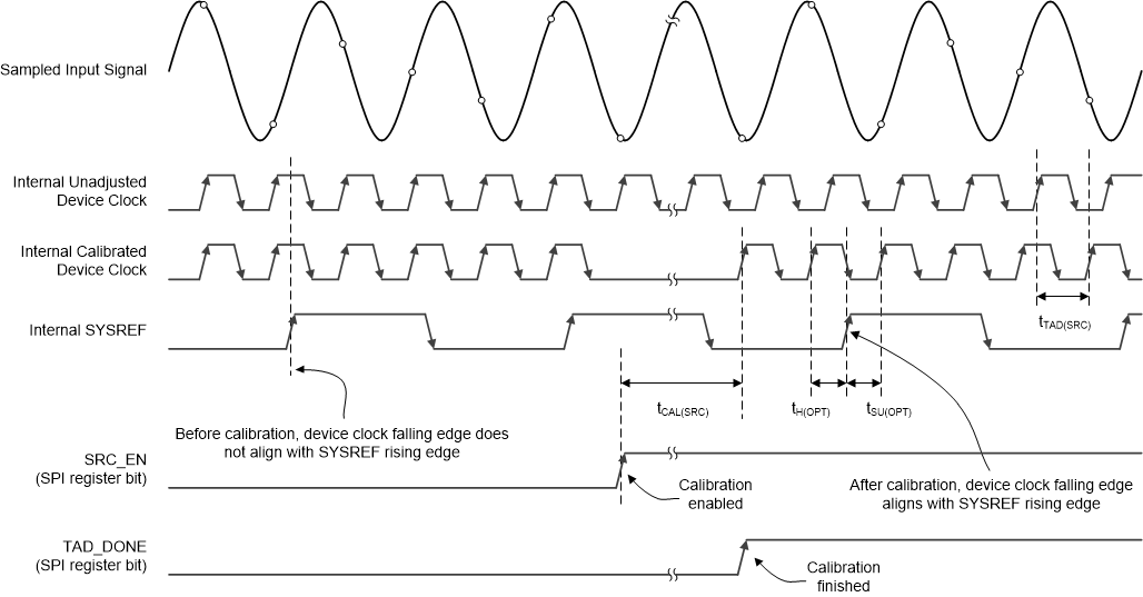
The device must have a proper device clock applied and be programmed for normal operation before starting the automatic SYSREF calibration. When ready to initiate automatic SYSREF calibration, a continuous SYSREF signal must be applied. SYSREF must be a continuous (periodic) signal when using the automatic SYSREF calibration. Start the calibration process by setting SRC_EN high in the SYSREF calibration enable register after configuring the automatic SYSREF calibration using the SRC_CFG register. Upon setting SRC_EN high, the device searches for the optimal tAD adjust setting until the device clock falling edge is internally aligned to the SYSREF rising edge. TAD_DONE in the SYSREF calibration status register can be monitored tomake sure the SYSREF calibration has finished. By aligning the device clock falling edge with the SYSREF rising edge, automatic SYSREF calibration maximizes the internal SYSREF setup and hold times relative to the device clock and also sets the sampling instant based on the SYSREF rising edge. After the automatic SYSREF calibration finishes, the rest of the startup procedure can be performed to finish bringing up the system.
For multi-device synchronization, the SYSREF rising edge timing must be matched at all devices and therefore trace lengths must be matched from a common SYSREF source to each device. Any skew between the SYSREF rising edge at each device results in additional error in the sampling instance between devices, however repeatable deterministic latency from system startup to startup through each device must still be achieved. No other design requirements are needed in order to achieve multi-device synchronization as long as a proper elastic buffer release point is chosen in the JESD204C receiver.
Figure 7-3 provides a timing diagram of the SYSREF calibration procedure. The optimized setup and hold times are shown as tSU(OPT) and tH(OPT), respectively. Device clock and SYSREF are referred to as internal in this diagram because the phase of the internal signals are aligned within the device and not to the external (applied) phase of the device clock or SYSREF.
 Figure 7-3 SYSREF Calibration Timing Diagram
When finished, the tAD adjust setting found by the automatic SYSREF calibration can be read from SRC_TAD in the SYSREF calibration status register. After calibration, the system continues to use the calibrated tAD adjust setting for operation until the system is powered down. However, if desired, the user can then disable the SYSREF calibration and fine-tune the tAD adjust setting according to the systems needs. Alternatively, the use of the automatic SYSREF calibration can be done at product test (or periodic recalibration) of the optimal tAD adjust setting for each system. This value can be stored and written to the TAD register (TAD_INV, TAD_COARSE, and TAD_FINE) upon system startup.
Do not run the SYSREF calibration when the ADC calibration (foreground or background) is running. If background calibration is the desired use case, disable the background calibration when the SYSREF calibration is used, then reenable the background calibration after TAD_DONE goes high. SYSREF_SEL in the clock control register 0 must be set to 0 when using SYSREF calibration.
SYSREF calibration searches the TAD_COARSE delays using both noninverted (TAD_INV = 0) and inverted clock polarity (TAD_INV = 1) to minimize the required TAD_COARSE setting in order to minimize loss on the clock path to reduce aperture jitter (tAJ).