JAJSLQ5C April 2021 – September 2022 ADS127L11
PRODUCTION DATA
- 1 特長
- 2 アプリケーション
- 3 概要
- 4 Revision History
- 5 Pin Configuration and Functions
-
6 Specifications
- 6.1 Absolute Maximum Ratings
- 6.2 ESD Ratings
- 6.3 Recommended Operating Conditions
- 6.4 Thermal Information
- 6.5 Electrical Characteristics
- 6.6 Timing Requirements (1.65 V ≤ IOVDD ≤ 2 V)
- 6.7 Switching Characteristics (1.65 V ≤ IOVDD ≤ 2 V)
- 6.8 Timing Requirements (2 V < IOVDD ≤ 5.5 V)
- 6.9 Switching Characteristics (2 V < IOVDD ≤ 5.5 V)
- 6.10 Timing Diagrams
- 6.11 Typical Characteristics
- 7 Parameter Measurement Information
-
8 Detailed Description
- 8.1 Overview
- 8.2 Functional Block Diagram
- 8.3 Feature Description
- 8.4 Device Functional Modes
- 8.5 Programming
- 8.6
Registers
- 8.6.1 DEV_ID Register (Address = 0h) [reset = 00h]
- 8.6.2 REV_ID Register (Address = 1h) [reset = xxh]
- 8.6.3 STATUS Register (Address = 2h) [reset = x1100xxxb]
- 8.6.4 CONTROL Register (Address = 3h) [reset = 00h]
- 8.6.5 MUX Register (Address = 4h) [reset = 00h]
- 8.6.6 CONFIG1 Register (Address = 5h) [reset = 00h]
- 8.6.7 CONFIG2 Register (Address = 6h) [reset = 00h]
- 8.6.8 CONFIG3 Register (Address = 7h) [reset = 00h]
- 8.6.9 CONFIG4 Register (Address = 8h) [reset = 00h]
- 8.6.10 OFFSET2, OFFSET1, OFFSET0 Registers (Addresses = 9h, Ah, Bh) [reset = 00h, 00h, 00h]
- 8.6.11 GAIN2, GAIN1, GAIN0 Registers (Addresses = Ch, Dh, Eh) [reset = 40h, 00h, 00h]
- 8.6.12 CRC Register (Address = Fh) [reset = 00h]
- 9 Application and Implementation
- 10Device and Documentation Support
- 11Mechanical, Packaging, and Orderable Information
パッケージ・オプション
メカニカル・データ(パッケージ|ピン)
サーマルパッド・メカニカル・データ
- RUK|20
発注情報
8.3.2 Reference Voltage (REFP, REFN)
A reference voltage is required for operation. The reference voltage input is differential, defined as: VREF = VREFP – VREFN, and applied to the REFP and REFN inputs. See the Section 8.3.2.1 section for details of the reference voltage operating range.
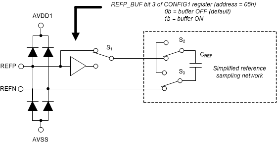
As shown in Figure 8-5, the reference inputs have an input structure similar to the analog inputs. ESD diodes protect the reference inputs. To keep these diodes from turning on, make sure the voltages on the reference pins do not go below AVSS by more than 0.3 V, or above AVDD1 by 0.3 V. If these conditions are possible, use external clamp diodes, series resistors, or both to limit the input current to the specified value.
 Figure 8-5 Reference Input
Circuit
Figure 8-5 Reference Input
CircuitThe reference voltage is sampled by a sampling capacitor CREF. In unbuffered mode, current flows through the reference inputs to charge the sampling capacitor. The current consists of a dc component and an ac component that varies with the frequency of the modulator sampling clock. See the Section 6.5 table for the reference input current specification.
The effect of charging the reference sampling capacitor requires the external reference driver to settle at the end of the sample phase t = 1 / (2 · fMOD). Incomplete settling of the reference voltage can lead to excessive gain error and gain error drift. Operation in low-speed mode reduces the modulator sampling clock frequency by 1/8th, therefore allowing more time for the reference driver to settle.
The ADC provides a precharge buffer option for the REFP input to reduce the charge drawn by the sampling capacitor. The precharge buffer provides the coarse charge for the reference sampling capacitor CREF. Halfway through the sample phase, the precharge buffer is bypassed (S1 is in an up position as demonstrated in Figure 8-5), at which time the external driver provides the fine charge to the sampling capacitor. Because the buffer reduces the charge demand of the sampling capacitor, the bandwidth requirement of the external driver is greatly reduced.
Many applications either ground REFN, or connect REFN to AVSS. A precharge buffer for REFN is not necessary for these cases. For applications when REFN is not a low impedance source, consider buffering the REFN input.