JAJSIY6C December 2011 – April 2020 ADS1291 , ADS1292 , ADS1292R
PRODUCTION DATA.
- 1 特長
- 2 アプリケーション
- 3 概要
- 4 改訂履歴
- 5 Pin Configuration and Functions
- 6 Specifications
- 7 Parameter Measurement Information
-
8 Detailed Description
- 8.1 Overview
- 8.2 Functional Block Diagram
- 8.3
Feature Description
- 8.3.1 EMI Filter
- 8.3.2
Input Multiplexer
- 8.3.2.1 Device Noise Measurements
- 8.3.2.2 Test Signals (TestP and TestN)
- 8.3.2.3 Auxiliary Differential Input (RESP_MODN/IN3N, RESP_MODN/IN3P)
- 8.3.2.4 Temperature Sensor (TEMPP, TEMPN)
- 8.3.2.5 Supply Measurements (MVDDP, MVDDN)
- 8.3.2.6 Lead-Off Excitation Signals (LoffP, LoffN)
- 8.3.2.7 Auxiliary Single-Ended Input
- 8.3.3 Analog Input
- 8.3.4 PGA Settings and Input Range
- 8.3.5 Digital Decimation Filter
- 8.3.6 Reference
- 8.3.7 Clock
- 8.3.8 Data Format
- 8.3.9 Multiple Device Configuration
- 8.3.10 ECG-Specific Functions
- 8.3.11 Setting the Device for Basic Data Capture
- 8.4 Device Functional Modes
- 8.5
Programming
- 8.5.1 SPI Interface
- 8.5.2
SPI Command Definitions
- 8.5.2.1 WAKEUP: Exit STANDBY Mode
- 8.5.2.2 STANDBY: Enter STANDBY Mode
- 8.5.2.3 RESET: Reset Registers to Default Values
- 8.5.2.4 START: Start Conversions
- 8.5.2.5 STOP: Stop Conversions
- 8.5.2.6 OFFSETCAL: Channel Offset Calibration
- 8.5.2.7 RDATAC: Read Data Continuous
- 8.5.2.8 SDATAC: Stop Read Data Continuous
- 8.5.2.9 RDATA: Read Data
- 8.5.2.10 Sending Multi-Byte Commands
- 8.5.2.11 RREG: Read From Register
- 8.5.2.12 WREG: Write to Register
- 8.6
Register Maps
- 8.6.1
User Register Description
- 8.6.1.1 ID: ID Control Register (Factory-Programmed, Read-Only) (address = 00h)
- 8.6.1.2 CONFIG1: Configuration Register 1 (address = 01h)
- 8.6.1.3 CONFIG2: Configuration Register 2 (address = 02h)
- 8.6.1.4 LOFF: Lead-Off Control Register (address = 03h)
- 8.6.1.5 CH1SET: Channel 1 Settings (address = 04h)
- 8.6.1.6 CH2SET: Channel 2 Settings (address = 05h)
- 8.6.1.7 RLD_SENS: Right Leg Drive Sense Selection (address = 06h)
- 8.6.1.8 LOFF_SENS: Lead-Off Sense Selection (address = 07h)
- 8.6.1.9 LOFF_STAT: Lead-Off Status (address = 08h)
- 8.6.1.10 RESP1: Respiration Control Register 1 (address = 09h)
- 8.6.1.11 RESP2: Respiration Control Register 2 (address = 0Ah)
- 8.6.1.12 GPIO: General-Purpose I/O Register (address = 0Bh)
- 8.6.1
User Register Description
- 9 Application and Implementation
- 10Power Supply Recommendations
- 11Layout
- 12デバイスおよびドキュメントのサポート
- 13メカニカル、パッケージ、および注文情報
パッケージ・オプション
メカニカル・データ(パッケージ|ピン)
サーマルパッド・メカニカル・データ
- PBS|32
発注情報
8.3.10.2.4 Right Leg Drive (RLD DC Bias Circuit)
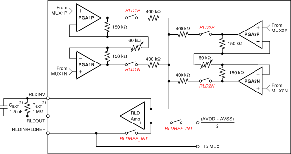
The right leg drive (RLD) circuitry is used as a means to counter the common-mode interference in a ECG system as a result of power lines and other sources, including fluorescent lights. The RLD circuit senses the common-mode of a selected set of electrodes and creates a negative feedback loop by driving the body with an inverted common-mode signal. The negative feedback loop restricts the common-mode movement to a narrow range, depending on the loop gain. Stabilizing the entire loop is specific to the individual user system based on the various poles in the loop. The ADS1291, ADS1292, and ADS1292R integrates the muxes to select the channel and an operational amplifier. All the amplifier terminals are available at the pins, allowing the user to choose the components for the feedback loop. The circuit shown in Figure 40 shows the overall functional connectivity for the RLD bias circuit.
The reference voltage for the right leg drive can be chosen to be internally generated (AVDD + AVSS) / 2 or it can be provided externally with a resistive divider. The selection of an internal versus external reference voltage for the RLD loop is defined by writing the appropriate value to the RLDREF_INT bit in the RESP2 register.

If the RLD function is not used, the amplifier can be powered down using the PDB_RLD bit. This bit is also used in daisy-chain mode to power-down all but one of the RLD amplifiers.
The functionality of the RLDIN pin is explained in the Input Multiplexer section.