SBAS590E March   2016  – June 2020 ADS131A02 , ADS131A04

PRODUCTION DATA.  

  1. Features
  2. Applications
  3. Description
    1.     Simplified Block Diagram
  4. Revision History
  5. Device Comparison Table
  6. Pin Configuration and Functions
    1.     Pin Functions
  7. Specifications
    1. 7.1  Absolute Maximum Ratings
    2. 7.2  ESD Ratings
    3. 7.3  Recommended Operating Conditions
    4. 7.4  Thermal Information
    5. 7.5  Electrical Characteristics
    6. 7.6  Timing Requirements: Asynchronous Interrupt Interface Mode
    7. 7.7  Switching Characteristics: Asynchronous Interrupt Interface Mode
    8. 7.8  Timing Requirements: Synchronous Master Interface Mode
    9. 7.9  Switching Characteristics: Synchronous Master Interface Mode
    10. 7.10 Timing Requirements: Synchronous Slave Interface Mode
    11. 7.11 Switching Characteristics: Synchronous Slave Interface Mode
    12. 7.12 Typical Characteristics
  8. Parameter Measurement Information
    1. 8.1 Noise Measurements
  9. Detailed Description
    1. 9.1 Overview
    2. 9.2 Functional Block Diagram
    3. 9.3 Feature Description
      1. 9.3.1 Clock
        1. 9.3.1.1 XTAL1/CLKIN and XTAL2
        2. 9.3.1.2 ICLK
        3. 9.3.1.3 MODCLK
        4. 9.3.1.4 Data Rate
      2. 9.3.2 Analog Input
      3. 9.3.3 Input Overrange and Underrange Detection
      4. 9.3.4 Reference
      5. 9.3.5 ΔΣ Modulator
      6. 9.3.6 Digital Decimation Filter
      7. 9.3.7 Watchdog Timer
    4. 9.4 Device Functional Modes
      1. 9.4.1 Low-Power and High-Resolution Mode
      2. 9.4.2 Power-Up
      3. 9.4.3 Standby and Wake-Up Mode
      4. 9.4.4 Conversion Mode
      5. 9.4.5 Reset (RESET)
    5. 9.5 Programming
      1. 9.5.1 Interface Protocol
        1. 9.5.1.1 Device Word Length
        2. 9.5.1.2 Fixed versus Dynamic-Frame Mode
        3. 9.5.1.3 Command Word
        4. 9.5.1.4 Status Word
        5. 9.5.1.5 Data Words
          1. 9.5.1.5.1 ADC Data Word 16-Bit Format
          2. 9.5.1.5.2 ADC Data Word 24-Bit Format
        6. 9.5.1.6 Hamming Code Error Correction
        7. 9.5.1.7 Cyclic Redundancy Check (CRC)
          1. 9.5.1.7.1 Computing the CRC
          2. 9.5.1.7.2 CRC With CRC_MODE = 1
          3. 9.5.1.7.3 CRC with CRC_MODE = 0
          4. 9.5.1.7.4 CRC Using the WREGS Command
      2. 9.5.2 SPI Interface
        1. 9.5.2.1 Asynchronous Interrupt Mode
          1. 9.5.2.1.1 Chip Select (CS)
          2. 9.5.2.1.2 Serial Clock (SCLK)
          3. 9.5.2.1.3 Data Input (DIN)
          4. 9.5.2.1.4 Data Output (DOUT)
          5. 9.5.2.1.5 Data Ready (DRDY)
          6. 9.5.2.1.6 Asynchronous Interrupt Mode Data Retrieval
        2. 9.5.2.2 Synchronous Master Mode
          1. 9.5.2.2.1 Serial Clock (SCLK)
          2. 9.5.2.2.2 Data Input (DIN)
          3. 9.5.2.2.3 Data Output (DOUT)
          4. 9.5.2.2.4 Data Ready (DRDY)
          5. 9.5.2.2.5 Chip Select (CS)
          6. 9.5.2.2.6 Synchronous Master Mode Data Retrieval
        3. 9.5.2.3 Synchronous Slave Mode
          1. 9.5.2.3.1 Chip Select (CS)
          2. 9.5.2.3.2 Serial Clock (SCLK)
          3. 9.5.2.3.3 Data Input (DIN)
          4. 9.5.2.3.4 Data Output (DOUT)
          5. 9.5.2.3.5 Data Ready (DRDY)
          6. 9.5.2.3.6 Synchronous Slave Mode Data Retrieval
        4. 9.5.2.4 ADC Frame Complete (DONE)
      3. 9.5.3 SPI Command Definitions
        1. 9.5.3.1  NULL: Null Command
        2. 9.5.3.2  RESET: Reset to POR Values
        3. 9.5.3.3  STANDBY: Enter Standby Mode
        4. 9.5.3.4  WAKEUP: Exit Standby Mode
        5. 9.5.3.5  LOCK: Lock ADC Registers
        6. 9.5.3.6  UNLOCK: Unlock ADC Registers
          1. 9.5.3.6.1 UNLOCK from POR or RESET
        7. 9.5.3.7  RREG: Read a Single Register
        8. 9.5.3.8  RREGS: Read Multiple Registers
        9. 9.5.3.9  WREG: Write Single Register
        10. 9.5.3.10 WREGS: Write Multiple Registers
    6. 9.6 Register Maps
      1. 9.6.1 User Register Description
        1. 9.6.1.1  ID_MSB: ID Control Register MSB (address = 00h) [reset = xxh]
          1. Table 16. ID_MSB Register Field Descriptions
        2. 9.6.1.2  ID_LSB: ID Control Register LSB (address = 01h) [reset = xxh]
          1. Table 17. ID_LSB Register Field Descriptions
        3. 9.6.1.3  STAT_1: Status 1 Register (address = 02h) [reset = 00h]
          1. Table 18. STAT_1 Register Field Descriptions
        4. 9.6.1.4  STAT_P: Positive Input Fault Detect Status Register (address = 03h) [reset = 00h]
          1. Table 19. STAT_P Register Field Descriptions
        5. 9.6.1.5  STAT_N: Negative Input Fault Detect Status Register (address = 04h) [reset = 00h]
          1. Table 20. STAT_N Register Field Descriptions
        6. 9.6.1.6  STAT_S: SPI Status Register (address = 05h) [reset = 00h]
          1. Table 21. STAT_S Register Field Descriptions
        7. 9.6.1.7  ERROR_CNT: Error Count Register (address = 06h) [reset = 00h]
          1. Table 22. ERROR_CNT Register Field Descriptions
        8. 9.6.1.8  STAT_M2: Hardware Mode Pin Status Register (address = 07h) [reset = xxh]
          1. Table 23. STAT_M2 Register Field Descriptions
        9. 9.6.1.9  Reserved Registers (address = 08h to 0Ah) [reset = 00h]
          1. Table 24. Reserved Registers Field Descriptions
        10. 9.6.1.10 A_SYS_CFG: Analog System Configuration Register (address = 0Bh) [reset = 60h]
          1. Table 25. A_SYS_CFG Register Field Descriptions
        11. 9.6.1.11 D_SYS_CFG: Digital System Configuration Register (address = 0Ch) [reset = 3Ch]
          1. Table 27. D_SYS_CFG Register Field Descriptions
        12. 9.6.1.12 CLK1: Clock Configuration 1 Register (address = 0Dh) [reset = 08h]
          1. Table 28. CLK1 Register Field Descriptions
        13. 9.6.1.13 CLK2: Clock Configuration 2 Register (address = 0Eh) [reset = 86h]
          1. Table 29. CLK2 Register Field Descriptions
        14. 9.6.1.14 ADC_ENA: ADC Channel Enable Register (address = 0Fh) [reset = 00h]
          1. Table 31. ADC_ENA Register Field Descriptions
        15. 9.6.1.15 Reserved Register (address = 10h) [reset = 00h]
          1. Table 32. Reserved Register Field Descriptions
      2. 9.6.2 ADCx: ADC Channel Digital Gain Configuration Registers (address = 11h to 14h) [reset = 00h]
        1. Table 33. ADCx Registers Field Descriptions
  10. 10Application and Implementation
    1. 10.1 Application Information
      1. 10.1.1 Unused Inputs and Outputs
      2. 10.1.2 Power Monitoring Specific Applications
      3. 10.1.3 Multiple Device Configuration
        1. 10.1.3.1 First Device Configured in Asynchronous Interrupt Mode
        2. 10.1.3.2 First Device Configured in Synchronous Master Mode
        3. 10.1.3.3 All Devices Configured in Synchronous Slave Mode
    2. 10.2 Typical Application
      1. 10.2.1 Design Requirements
      2. 10.2.2 Detailed Design Procedure
      3. 10.2.3 Application Curve
    3. 10.3 What To Do and What Not To Do
    4. 10.4 Initialization Set Up
  11. 11Power Supply Recommendations
    1. 11.1 Negative Charge Pump
    2. 11.2 Internal Digital LDO
    3. 11.3 Power-Supply Sequencing
    4. 11.4 Power-Supply Decoupling
  12. 12Layout
    1. 12.1 Layout Guidelines
    2. 12.2 Layout Example
  13. 13Device and Documentation Support
    1. 13.1 Documentation Support
      1. 13.1.1 Related Documentation
    2. 13.2 Related Links
    3. 13.3 Receiving Notification of Documentation Updates
    4. 13.4 Support Resources
    5. 13.5 Trademarks
    6. 13.6 Electrostatic Discharge Caution
    7. 13.7 Glossary
  14. 14Mechanical, Packaging, and Orderable Information

パッケージ・オプション

デバイスごとのパッケージ図は、PDF版データシートをご参照ください。

メカニカル・データ(パッケージ|ピン)
  • PBS|32
サーマルパッド・メカニカル・データ
発注情報

First Device Configured in Synchronous Master Mode

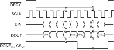
Figure 98 shows a multiple device configuration where the first device is configured in synchronous master mode as indicated by the state of the M0 pin. The second ADS131A0x device and any additional devices are configured in synchronous slave mode. The DONE pin of each device connects to the CS pin of the subsequent device. In each case, after a device shifts out all of its data, the device deasserts DONE, selecting the subsequent device for communication. Tie the DONE pin of the last device to the CS pin of the first device to allow for an immediate second read back of conversion data in the case a data integrity test failed. The DOUT of a device whose contents are already shifted out assumes a high-impedance state, allowing the DOUT pins of all devices to be tied together. To send commands to specific devices, send the respective command of the device when that device is selected for communication. The DRDY output of the first device serves as the DRDY input to all other devices to synchronize conversions. DRDY also serves as the chip-select or frame sync signal for the host. SCLK is free running with the same frequency as ICLK in this configuration. Figure 99 illustrates an example interface timing diagram for this configuration.
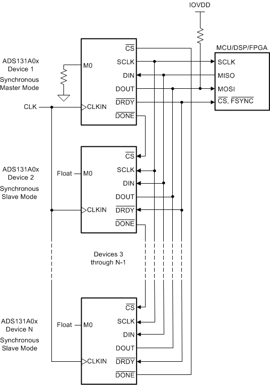
ADS131A02 ADS131A04 apps_syncM_chain_sbas590.gifFigure 98. Multiple Device Configuration Using Synchronous Master Mode
ADS131A02 ADS131A04 apps_syncM_chain_timing_sbas590.gif

NOTE:

(1) denotes device 1, (2) denotes device 2, and (N) denotes device N.
Figure 99. Multiple Device Configuration Timing Diagram When Using Synchronous Master Mode