JAJSIU8B June 2015 – April 2020 ADS131E08S
PRODUCTION DATA.
- 1 特長
- 2 アプリケーション
- 3 説明
- 4 改訂履歴
- 5 Device Comparison
- 6 Pin Configuration and Functions
- 7 Specifications
- 8 Parameter Measurement Information
-
9 Detailed Description
- 9.1 Overview
- 9.2 Functional Block Diagram
- 9.3 Feature Description
- 9.4 Device Functional Modes
- 9.5
Programming
- 9.5.1 SPI Interface
- 9.5.2 Data Retrieval
- 9.5.3
SPI Command Definitions
- 9.5.3.1 WAKEUP: Exit STANDBY Mode
- 9.5.3.2 STANDBY: Enter STANDBY Mode
- 9.5.3.3 RESET: Reset Registers to Default Values
- 9.5.3.4 START: Start Conversions
- 9.5.3.5 STOP: Stop Conversions
- 9.5.3.6 OFFSETCAL: Channel Offset Calibration
- 9.5.3.7 RDATAC: Start Read Data Continuous Mode
- 9.5.3.8 SDATAC: Stop Read Data Continuous Mode
- 9.5.3.9 RDATA: Read Data
- 9.5.3.10 RREG: Read from Register
- 9.5.3.11 WREG: Write to Register
- 9.5.3.12 Sending Multibyte Commands
- 9.6
Register Map
- 9.6.1
Register Descriptions
- 9.6.1.1 ID: ID Control Register (Factory-Programmed, Read-Only) (address = 00h) [reset = D2h]
- 9.6.1.2 CONFIG1: Configuration Register 1 (address = 01h) [reset = 94h]
- 9.6.1.3 CONFIG2: Configuration Register 2 (address = 02h) [reset = 00h]
- 9.6.1.4 CONFIG3: Configuration Register 3 (address = 03h) [reset = E0h]
- 9.6.1.5 FAULT: Fault Detect Control Register (address = 04h) [reset = 00h]
- 9.6.1.6 CHnSET: Individual Channel Settings (address = 05h to 0Ch) [reset = 10h]
- 9.6.1.7 FAULT_STATP: Fault Detect Positive Input Status (address = 12h) [reset = 00h]
- 9.6.1.8 FAULT_STATN: Fault Detect Negative Input Status (address = 13h) [reset = 00h]
- 9.6.1.9 GPIO: General-Purpose IO Register (address = 14h) [reset = 0Fh]
- 9.6.1
Register Descriptions
- 10Application and Implementation
- 11Power Supply Recommendations
- 12Layout
- 13デバイスおよびドキュメントのサポート
- 14メカニカル、パッケージ、および注文情報
10.1.1.3 Daisy-Chain Configuration
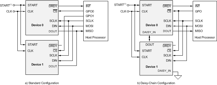
Daisy-chain mode is enabled by setting the DAISY_IN bit in the CONFIG1 register. Figure 55b shows the daisy-chain configuration. In this mode SCLK, DIN, and CS are shared across multiple devices. The DOUT pin of device 1 is connected to the DAISY_IN pin of device 0, thereby creating a daisy-chain for the data. Connect the DAISY_IN pin of device 1 to DGND if not used. The daisy-chain timing requirements for the SPI interface are illustrated in Figure 2. Data from the ADS131E08S device 0 appear first on DOUT, followed by a don’t care bit, and then the status and data words from the ADS131E08S device 1.
The internal oscillator output cannot be enabled because all devices in the chain operate by sharing the same DIN pin, thus an external clock must be used.

There are several items to be aware of when using daisy-chain mode:
- One extra SCLK must be issued between each data set (see Figure 56)
- All devices are configured to the same register values because the CS signal is shared
- Device register readback is only valid for device 0 in the daisy-chain. Only ADC conversion data can be read back from device 1 through device N, where N is the last device in the chain.
The more devices in the chain, the more challenging adhering to setup and hold times becomes. A star-pattern connection of SCLK to all devices, minimizing the trace length of DOUT, and other printed circuit board (PCB) layout techniques helps to mitigate this challenge with signal delays. Placing delay circuits (such as buffers) between DOUT and DAISY_IN are options to help reduce signal delays. One other option is to insert a D flip-flop between DOUT and DAISY_IN clocked on an inverted SCLK. Figure 56 shows a timing diagram for daisy-chain mode.

NOTE:
n = (number of channels) × (resolution) + 24 bits. The number of channels is 8. Resolution is 16 bits or 24 bits.The maximum number of devices that can be daisy-chained depends on the data rate that the devices are operated at. The maximum number of devices can be calculated with Equation 10.

where
- NBITS = device resolution (depends on DR[2:0] setting)
- NCHANNELS = number of channels powered up in the device
For example, when the ADS131E08S is operated in 24-bit, 8-kSPS data rate with fSCLK = 10 MHz, up to six devices can be daisy-chained together.