JAJSI11B October 2019 – February 2021 ADS131M08
PRODUCTION DATA
- 1 特長
- 2 アプリケーション
- 3 概要
- 4 Revision History
- 5 Pin Configuration and Functions
- 6 Specifications
- 7 Parameter Measurement Information
-
8 Detailed Description
- 8.1 Overview
- 8.2 Functional Block Diagram
- 8.3
Feature Description
- 8.3.1 Input ESD Protection Circuitry
- 8.3.2 Input Multiplexer
- 8.3.3 Programmable Gain Amplifier (PGA)
- 8.3.4 Voltage Reference
- 8.3.5 Clocking and Power Modes
- 8.3.6 ΔΣ Modulator
- 8.3.7 Digital Filter
- 8.3.8 DC Block Filter
- 8.3.9 Internal Test Signals
- 8.3.10 Channel Phase Calibration
- 8.3.11 Calibration Registers
- 8.3.12 Communication Cyclic Redundancy Check (CRC)
- 8.3.13 Register Map CRC
- 8.4 Device Functional Modes
- 8.5
Programming
- 8.5.1
Interface
- 8.5.1.1 Chip Select (CS)
- 8.5.1.2 Serial Data Clock (SCLK)
- 8.5.1.3 Serial Data Input (DIN)
- 8.5.1.4 Serial Data Output (DOUT)
- 8.5.1.5 Data Ready (DRDY)
- 8.5.1.6 Conversion Synchronization or System Reset (SYNC/RESET)
- 8.5.1.7 SPI Communication Frames
- 8.5.1.8 SPI Communication Words
- 8.5.1.9 ADC Conversion Data
- 8.5.1.10
Commands
- 8.5.1.10.1 NULL (0000 0000 0000 0000)
- 8.5.1.10.2 RESET (0000 0000 0001 0001)
- 8.5.1.10.3 STANDBY (0000 0000 0010 0010)
- 8.5.1.10.4 WAKEUP (0000 0000 0011 0011)
- 8.5.1.10.5 LOCK (0000 0101 0101 0101)
- 8.5.1.10.6 UNLOCK (0000 0110 0110 0110)
- 8.5.1.10.7 RREG (101a aaaa annn nnnn)
- 8.5.1.10.8 WREG (011a aaaa annn nnnn)
- 8.5.1.11 Short SPI Frames
- 8.5.2 Synchronization
- 8.5.1
Interface
- 8.6 Registers
- 9 Application and Implementation
- 10Power Supply Recommendations
- 11Layout
- 12Device and Documentation Support
- 13Mechanical, Packaging, and Orderable Information
パッケージ・オプション
メカニカル・データ(パッケージ|ピン)
サーマルパッド・メカニカル・データ
発注情報
9.2.2.5 Formulae
This section describes the formulas used for the power and energy calculations. Voltage and current samples are obtained at a sampling rate of 8000 Hz. All samples that are taken in approximately one-second (1 sec) frames are kept and used to obtain the RMS values for voltage and current for each phase.
Power and energy are calculated for active and reactive energy samples of one frame. These samples are phase-corrected. Then phase active and reactive powers are calculated through the following formulas:
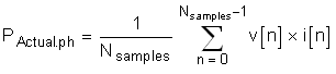
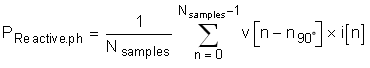
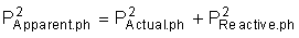
where:
- v[n] = Voltage sample
- i[n] = Current sample
- Nsamples = Number of samples in the approximately 1-second frame
- v[n-n90°] = Voltage sample with a 90° phase shift
- PACTUAL,ph = Instantaneous actual power for the measured phase
- PREACTIVE = Instantaneous reactive power for the measured phase
- PAPPARENT,ph = Instantaneous apparent power for the measured phase
The 90° phase shift approach is used for two reasons:
- This approach allows accurate measurement of the reactive power for very small currents
- This approach conforms to the measurement method specified by IEC and ANSI standards
The calculated mains frequency is used to calculate the 90° shifted voltage sample. Because the frequency of the mains varies, the mains frequency is first measured accurately to phase shift the voltage samples accordingly.
To get an exact 90° phase shift, interpolation is used between two samples. For these two samples, a voltage sample slightly more than 90 degrees before the current sample and a voltage sample slightly less than 90° before the current sample are used. The phase shift implementation of the application consists of an integer part and a fractional part. The integer part is realized by providing an N samples delay. The fractional part is realized by a one-tap FIR filter.
The cumulative power values can be calculated by summing the per phase power results. The cumulative energy can be calculated by multiplying the cumulative power by the number of samples in the packet.
The host calculates the frequency in terms of samples-per-mains cycle by counting zero crossings of the sine wave. Equation 17 converts this result from a samples-per-mains cycle to Hertz.
After the active power and apparent power are calculated, the absolute value of the power factor is calculated. In the internal representation of power factor of the system, a positive power factor corresponds to a capacitive load and a negative power factor corresponds to an inductive load. The sign of the internal representation of power factor is determined by whether the current leads or lags voltage, which is determined in the background process. Therefore, Equation 18 and Equation 19 calculate the internal representation of the power factor: