JAJSHC9B May 2019 – October 2021 ALM2402F-Q1
PRODUCTION DATA
- 1 特長
- 2 アプリケーション
- 3 概要
- 4 Revision History
- 5 Pin Configuration and Functions
- 6 Specifications
- 7 Detailed Description
- 8 Application and Implementation
- 9 Power Supply Recommendations
- 10Layout
- 11Device and Documentation Support
- 12Mechanical, Packaging, and Orderable Information
パッケージ・オプション
メカニカル・データ(パッケージ|ピン)
- PWP|14
サーマルパッド・メカニカル・データ
- PWP|14
発注情報
8.1.1 Capacitive Load and Stability
The ALM2402F-Q1 is designed to be used in applications where driving a capacitive load is required. As with all op amps, specific instances can occur where the ALM2402F-Q1 device can become unstable. The particular op-amp circuit configuration, layout, gain, and output loading are some of the factors to consider when establishing whether or not an amplifier is stable in operation. An op amp in the unity-gain (1 V/V) buffer configuration that drives a capacitive load exhibits a greater tendency to be unstable than an amplifier operated at a higher-noise gain. The capacitive load, in conjunction with the op-amp output resistance, creates a pole within the feedback loop that degrades the phase margin. The degradation of the phase margin increases as the capacitive loading increases. When operating in the unity-gain configuration, the ALM2402F-Q1 remains stable with a pure capacitive load up to approximately 1 nF. Increasing the amplifier closed-loop gain allows the amplifier to drive increasingly larger capacitance. This increased capability is evident when observing the overshoot response of the amplifier at higher voltage gains.
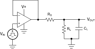
One technique for increasing the capacitive load drive capability of the amplifier operating in a unity-gain configuration is to insert a small resistor, typically 100 mΩ to 10 Ω, in series with the output (RS), as shown in Figure 8-1. This resistor significantly reduces the overshoot and ringing associated with large capacitive loads.
 Figure 8-1 Capacitive Load Drive