JAJSDZ0J October 2011 – April 2016 AM3351 , AM3352 , AM3354 , AM3356 , AM3357 , AM3358 , AM3359
PRODUCTION DATA.
- 1デバイスの概要
- 2改訂履歴
- 3Device Comparison
- 4Terminal Configuration and Functions
-
5Specifications
- 5.1 Absolute Maximum Ratings
- 5.2 ESD Ratings
- 5.3 Power-On Hours (POH)
- 5.4 Operating Performance Points (OPPs)
- 5.5 Recommended Operating Conditions
- 5.6 Power Consumption Summary
- 5.7 DC Electrical Characteristics
- 5.8 Thermal Resistance Characteristics for ZCE and ZCZ Packages
- 5.9 External Capacitors
- 5.10 Touch Screen Controller and Analog-to-Digital Subsystem Electrical Parameters
- 6Power and Clocking
-
7Peripheral Information and Timings
- 7.1 Parameter Information
- 7.2 Recommended Clock and Control Signal Transition Behavior
- 7.3 OPP50 Support
- 7.4 Controller Area Network (CAN)
- 7.5 DMTimer
- 7.6 Ethernet Media Access Controller (EMAC) and Switch
- 7.7
External Memory Interfaces
- 7.7.1 General-Purpose Memory Controller (GPMC)
- 7.7.2
mDDR(LPDDR), DDR2, DDR3, DDR3L Memory Interface
- 7.7.2.1 mDDR (LPDDR) Routing Guidelines
- 7.7.2.2
DDR2 Routing Guidelines
- 7.7.2.2.1 Board Designs
- 7.7.2.2.2
DDR2 Interface
- 7.7.2.2.2.1 DDR2 Interface Schematic
- 7.7.2.2.2.2 Compatible JEDEC DDR2 Devices
- 7.7.2.2.2.3 PCB Stackup
- 7.7.2.2.2.4 Placement
- 7.7.2.2.2.5 DDR2 Keepout Region
- 7.7.2.2.2.6 Bulk Bypass Capacitors
- 7.7.2.2.2.7 High-Speed (HS) Bypass Capacitors
- 7.7.2.2.2.8 Net Classes
- 7.7.2.2.2.9 DDR2 Signal Termination
- 7.7.2.2.2.10 DDR_VREF Routing
- 7.7.2.2.3 DDR2 CK and ADDR_CTRL Routing
- 7.7.2.3
DDR3 and DDR3L Routing Guidelines
- 7.7.2.3.1 Board Designs
- 7.7.2.3.2 DDR3 Device Combinations
- 7.7.2.3.3
DDR3 Interface
- 7.7.2.3.3.1 DDR3 Interface Schematic
- 7.7.2.3.3.2 Compatible JEDEC DDR3 Devices
- 7.7.2.3.3.3 PCB Stackup
- 7.7.2.3.3.4 Placement
- 7.7.2.3.3.5 DDR3 Keepout Region
- 7.7.2.3.3.6 Bulk Bypass Capacitors
- 7.7.2.3.3.7 High-Speed Bypass Capacitors
- 7.7.2.3.3.8 Net Classes
- 7.7.2.3.3.9 DDR3 Signal Termination
- 7.7.2.3.3.10 DDR_VREF Routing
- 7.7.2.3.3.11 VTT
- 7.7.2.3.4 DDR3 CK and ADDR_CTRL Topologies and Routing Definition
- 7.7.2.3.5 Data Topologies and Routing Definition
- 7.7.2.3.6 Routing Specification
- 7.8 I2C
- 7.9 JTAG Electrical Data and Timing
- 7.10 LCD Controller (LCDC)
- 7.11 Multichannel Audio Serial Port (McASP)
- 7.12 Multichannel Serial Port Interface (McSPI)
- 7.13 Multimedia Card (MMC) Interface
- 7.14 Programmable Real-Time Unit Subsystem and Industrial Communication Subsystem (PRU-ICSS)
- 7.15 Universal Asynchronous Receiver Transmitter (UART)
- 8Device and Documentation Support
- 9Mechanical, Packaging, and Orderable Information
パッケージ・オプション
デバイスごとのパッケージ図は、PDF版データシートをご参照ください。
メカニカル・データ(パッケージ|ピン)
- ZCZ|324
- ZCE|298
サーマルパッド・メカニカル・データ
発注情報
7 Peripheral Information and Timings
The AM335x device contains many peripheral interfaces. In order to reduce package size and lower overall system cost while maintaining maximum functionality, many of the AM335x terminals can multiplex up to eight signal functions. Although there are many combinations of pin multiplexing that are possible, only a certain number of sets, called I/O Sets, are valid due to timing limitations. These valid I/O Sets were carefully chosen to provide many possible application scenarios for the user.
Texas Instruments has developed a Windows-based application called Pin Mux Utility that helps a system designer select the appropriate pin-multiplexing configuration for their AM335x-based product design. The Pin Mux Utility provides a way to select valid I/O Sets of specific peripheral interfaces to ensure the pin-multiplexing configuration selected for a design only uses valid I/O Sets supported by the AM335x device.
7.1 Parameter Information
The data provided in the following Timing Requirements and Switching Characteristics tables assumes the device is operating within the Recommended Operating Conditions defined in Section 5, unless otherwise noted.
7.1.1 Timing Parameters and Board Routing Analysis
The timing parameter values specified in this data manual do not include delays by board routings. As a good board design practice, such delays must always be taken into account. Timing values may be adjusted by increasing or decreasing such delays. TI recommends using the available I/O buffer information specification (IBIS) models to analyze the timing characteristics correctly. If needed, external logic hardware such as buffers may be used to compensate any timing differences.
The timing parameter values specified in this data manual assume the SLEWCTRL bit in each pad control register is configured for fast mode (0b).
For the mDDR(LPDDR), DDR2, DDR3, DDR3L memory interface, it is not necessary to use the IBIS models to analyze timing characteristics. TI provides a PCB routing rules solution that describes the routing rules to ensure the mDDR(LPDDR), DDR2, DDR3, DDR3L memory interface timings are met.
7.2 Recommended Clock and Control Signal Transition Behavior
All clocks and control signals must transition between VIH and VIL (or between VIL and VIH) in a monotonic manner.
7.3 OPP50 Support
Some peripherals and features have limited support when the device is operating in OPP50. A complete list of these limitations follows.
| Not supported when operating in OPP50: | Reduced performance when operating in OPP50: |
|
|
7.4 Controller Area Network (CAN)
For more information, see the Controller Area Network (CAN) section of the AM335x and AMIC110 Sitara Processors Technical Reference Manual.
7.4.1 DCAN Electrical Data and Timing
Table 7-1 Timing Requirements for DCANx Receive
(see Figure 7-1)| NO. | MIN | MAX | UNIT | ||
|---|---|---|---|---|---|
| ƒbaud(baud) | Maximum programmable baud rate | 1 | Mbps | ||
| 1 | tw(RX) | Pulse duration, receive data bit | H – 2(1) | H + 2(1) | ns |
- H = Period of baud rate, 1 / programmed baud rate
Table 7-2 Switching Characteristics for DCANx Transmit
(see Figure 7-1)| NO. | PARAMETER | MIN | MAX | UNIT | |
|---|---|---|---|---|---|
| ƒbaud(baud) | Maximum programmable baud rate | 1 | Mbps | ||
| 2 | tw(TX) | Pulse duration, transmit data bit | H – 2(1) | H + 2(1) | ns |
- H = Period of baud rate, 1 / programmed baud rate
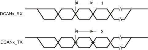 Figure 7-1 DCANx Timings
7.5 DMTimer
7.5.1 DMTimer Electrical Data and Timing
Table 7-3 Timing Requirements for DMTimer [1-7]
(see Figure 7-2)| NO. | MIN | MAX | UNIT | ||
|---|---|---|---|---|---|
| 1 | tc(TCLKIN) | Cycle time, TCLKIN | 4P + 1(1) | ns | |
Table 7-4 Switching Characteristics for DMTimer [4-7]
(see Figure 7-2)| NO. | PARAMETER | MIN | MAX | UNIT | |
|---|---|---|---|---|---|
| 2 | tw(TIMERxH) | Pulse duration, high | 4P – 3(1) | ns | |
| 3 | tw(TIMERxL) | Pulse duration, low | 4P – 3(1) | ns | |
 Figure 7-2 Timer Timing
7.6 Ethernet Media Access Controller (EMAC) and Switch
7.6.1 EMAC and Switch Electrical Data and Timing
The EMAC and Switch implemented in the AM335x device supports GMII mode, but the AM335x design does not pin out 9 of the 24 GMII signals. This was done to reduce the total number of package terminals. Therefore, the AM335x device does not support GMII mode. MII mode is supported with the remaining GMII signals.
The AM335x and AMIC110 Sitara Processors Technical Reference Manual and this document may reference internal signal names when discussing peripheral input and output signals because many of the AM335x package terminals can be multiplexed to one of several peripheral signals. For example, the AM335x terminal names for port 1 of the EMAC and switch have been changed from GMII to MII to indicate their Mode 0 function, but the internal signal is named GMII. However, documents that describe the Ethernet switch reference these signals by their internal signal name. For a cross-reference of internal signal names to terminal names, see Table 4-2.
Operation of the EMAC and switch is not supported for OPP50.
Table 7-5 EMAC and Switch Timing Conditions
| PARAMETER | MIN | TYP | MAX | UNIT | |
|---|---|---|---|---|---|
| Input Conditions | |||||
| tR | Input signal rise time | 1(1) | 5(1) | ns | |
| tF | Input signal fall time | 1(1) | 5(1) | ns | |
| Output Condition | |||||
| CLOAD | Output load capacitance | 3 | 30 | pF | |
- Except when specified otherwise.
7.6.1.1 EMAC/Switch MDIO Electrical Data and Timing
Table 7-6 Timing Requirements for MDIO_DATA
(see Figure 7-3)| NO. | MIN | TYP | MAX | UNIT | ||
|---|---|---|---|---|---|---|
| 1 | tsu(MDIO-MDC) | Setup time, MDIO valid before MDC high | 90 | ns | ||
| 2 | th(MDIO-MDC) | Hold time, MDIO valid from MDC high | 0 | ns | ||
 Figure 7-3 MDIO_DATA Timing - Input Mode
Table 7-7 Switching Characteristics for MDIO_CLK
(see Figure 7-4)| NO. | PARAMETER | MIN | TYP | MAX | UNIT | |
|---|---|---|---|---|---|---|
| 1 | tc(MDC) | Cycle time, MDC | 400 | ns | ||
| 2 | tw(MDCH) | Pulse duration, MDC high | 160 | ns | ||
| 3 | tw(MDCL) | Pulse duration, MDC low | 160 | ns | ||
| 4 | tt(MDC) | Transition time, MDC | 5 | ns | ||
 Figure 7-4 MDIO_CLK Timing
Table 7-8 Switching Characteristics for MDIO_DATA
(see Figure 7-5)| NO. | PARAMETER | MIN | TYP | MAX | UNIT | |
|---|---|---|---|---|---|---|
| 1 | td(MDC-MDIO) | Delay time, MDC high to MDIO valid | 10 | 390 | ns | |
 Figure 7-5 MDIO_DATA Timing - Output Mode
7.6.1.2 EMAC and Switch MII Electrical Data and Timing
Table 7-9 Timing Requirements for GMII[x]_RXCLK - MII Mode
(see Figure 7-6)| NO. | 10 Mbps | 100 Mbps | UNIT | ||||||
|---|---|---|---|---|---|---|---|---|---|
| MIN | TYP | MAX | MIN | TYP | MAX | ||||
| 1 | tc(RX_CLK) | Cycle time, RX_CLK | 399.96 | 400.04 | 39.996 | 40.004 | ns | ||
| 2 | tw(RX_CLKH) | Pulse duration, RX_CLK high | 140 | 260 | 14 | 26 | ns | ||
| 3 | tw(RX_CLKL) | Pulse duration, RX_CLK low | 140 | 260 | 14 | 26 | ns | ||
| 4 | tt(RX_CLK) | Transition time, RX_CLK | 5 | 5 | ns | ||||
![AM3359 AM3358 AM3357 AM3356 AM3354 AM3352 AM3351 GMII[x]_RXCLK Timing -
MII Mode AM3359 AM3358 AM3357 AM3356 AM3354 AM3352 AM3351 td_emac_rxclk_sprs717.gif](/ods/images/JAJSDZ0J/td_emac_rxclk_sprs717.gif) Figure 7-6 GMII[x]_RXCLK Timing - MII Mode
Figure 7-6 GMII[x]_RXCLK Timing - MII Mode
Table 7-10 Timing Requirements for GMII[x]_TXCLK - MII Mode
(see Figure 7-7)| NO. | 10 Mbps | 100 Mbps | UNIT | ||||||
|---|---|---|---|---|---|---|---|---|---|
| MIN | TYP | MAX | MIN | TYP | MAX | ||||
| 1 | tc(TX_CLK) | Cycle time, TX_CLK | 399.96 | 400.04 | 39.996 | 40.004 | ns | ||
| 2 | tw(TX_CLKH) | Pulse duration, TX_CLK high | 140 | 260 | 14 | 26 | ns | ||
| 3 | tw(TX_CLKL) | Pulse duration, TX_CLK low | 140 | 260 | 14 | 26 | ns | ||
| 4 | tt(TX_CLK) | Transition time, TX_CLK | 5 | 5 | ns | ||||
![AM3359 AM3358 AM3357 AM3356 AM3354 AM3352 AM3351 GMII[x]_TXCLK Timing -
MII Mode AM3359 AM3358 AM3357 AM3356 AM3354 AM3352 AM3351 td_emac_txclk_sprs717.gif](/ods/images/JAJSDZ0J/td_emac_txclk_sprs717.gif) Figure 7-7 GMII[x]_TXCLK Timing - MII Mode
Figure 7-7 GMII[x]_TXCLK Timing - MII Mode
Table 7-11 Timing Requirements for GMII[x]_RXD[3:0], GMII[x]_RXDV, and GMII[x]_RXER - MII Mode
(see Figure 7-8)| NO. | 10 Mbps | 100 Mbps | UNIT | ||||||
|---|---|---|---|---|---|---|---|---|---|
| MIN | TYP | MAX | MIN | TYP | MAX | ||||
| 1 | tsu(RXD-RX_CLK) | Setup time, RXD[3:0] valid before RX_CLK | 8 | 8 | ns | ||||
| tsu(RX_DV-RX_CLK) | Setup time, RX_DV valid before RX_CLK | ||||||||
| tsu(RX_ER-RX_CLK) | Setup time, RX_ER valid before RX_CLK | ||||||||
| 2 | th(RX_CLK-RXD) | Hold time RXD[3:0] valid after RX_CLK | 8 | 8 | ns | ||||
| th(RX_CLK-RX_DV) | Hold time RX_DV valid after RX_CLK | ||||||||
| th(RX_CLK-RX_ER) | Hold time RX_ER valid after RX_CLK | ||||||||
Table 7-12 Switching Characteristics for GMII[x]_TXD[3:0], and GMII[x]_TXEN - MII Mode
(see Figure 7-9)| NO. | PARAMETER | 10 Mbps | 100 Mbps | UNIT | |||||
|---|---|---|---|---|---|---|---|---|---|
| MIN | TYP | MAX | MIN | TYP | MAX | ||||
| 1 | td(TX_CLK-TXD) | Delay time, TX_CLK high to TXD[3:0] valid | 5 | 25 | 5 | 25 | ns | ||
| td(TX_CLK-TX_EN) | Delay time, TX_CLK to TX_EN valid | ||||||||
7.6.1.3 EMAC and Switch RMII Electrical Data and Timing
Table 7-13 Timing Requirements for RMII[x]_REFCLK - RMII Mode
(see Figure 7-10)| NO. | MIN | TYP | MAX | UNIT | ||
|---|---|---|---|---|---|---|
| 1 | tc(REF_CLK) | Cycle time, REF_CLK | 19.999 | 20.001 | ns | |
| 2 | tw(REF_CLKH) | Pulse duration, REF_CLK high | 7 | 13 | ns | |
| 3 | tw(REF_CLKL) | Pulse duration, REF_CLK low | 7 | 13 | ns | |
![AM3359 AM3358 AM3357 AM3356 AM3354 AM3352 AM3351 RMII[x]_REFCLK Timing -
RMII Mode AM3359 AM3358 AM3357 AM3356 AM3354 AM3352 AM3351 td_emac_refclk_sprs717.gif](/ods/images/JAJSDZ0J/td_emac_refclk_sprs717.gif) Figure 7-10 RMII[x]_REFCLK Timing - RMII Mode
Figure 7-10 RMII[x]_REFCLK Timing - RMII Mode
Table 7-14 Timing Requirements for RMII[x]_RXD[1:0], RMII[x]_CRS_DV, and RMII[x]_RXER - RMII Mode
(see Figure 7-11)| NO. | MIN | TYP | MAX | UNIT | ||
|---|---|---|---|---|---|---|
| 1 | tsu(RXD-REF_CLK) | Setup time, RXD[1:0] valid before REF_CLK | 4 | ns | ||
| tsu(CRS_DV-REF_CLK) | Setup time, CRS_DV valid before REF_CLK | |||||
| tsu(RX_ER-REF_CLK) | Setup time, RX_ER valid before REF_CLK | |||||
| 2 | th(REF_CLK-RXD) | Hold time RXD[1:0] valid after REF_CLK | 2 | ns | ||
| th(REF_CLK-CRS_DV) | Hold time, CRS_DV valid after REF_CLK | |||||
| th(REF_CLK-RX_ER) | Hold time, RX_ER valid after REF_CLK | |||||
Table 7-15 Switching Characteristics for RMII[x]_TXD[1:0], and RMII[x]_TXEN - RMII Mode
(see Figure 7-12)| NO. | PARAMETER | MIN | TYP | MAX | UNIT | |
|---|---|---|---|---|---|---|
| 1 | td(REF_CLK-TXD) | Delay time, REF_CLK high to TXD[1:0] valid | 2 | 13 | ns | |
| td(REF_CLK-TXEN) | Delay time, REF_CLK to TXEN valid | |||||
| 2 | tr(TXD) | Rise time, TXD outputs | 1 | 5 | ns | |
| tr(TX_EN) | Rise time, TX_EN output | |||||
| 3 | tf(TXD) | Fall time, TXD outputs | 1 | 5 | ns | |
| tf(TX_EN) | Fall time, TX_EN output | |||||
7.6.1.4 EMAC and Switch RGMII Electrical Data and Timing
Table 7-16 Timing Requirements for RGMII[x]_RCLK - RGMII Mode
(see Figure 7-13)| NO. | 10 Mbps | 100 Mbps | 1000 Mbps | UNIT | ||||||||
|---|---|---|---|---|---|---|---|---|---|---|---|---|
| MIN | TYP | MAX | MIN | TYP | MAX | MIN | TYP | MAX | ||||
| 1 | tc(RXC) | Cycle time, RXC | 360 | 440 | 36 | 44 | 7.2 | 8.8 | ns | |||
| 2 | tw(RXCH) | Pulse duration, RXC high | 160 | 240 | 16 | 24 | 3.6 | 4.4 | ns | |||
| 3 | tw(RXCL) | Pulse duration, RXC low | 160 | 240 | 16 | 24 | 3.6 | 4.4 | ns | |||
| 4 | tt(RXC) | Transition time, RXC | 0.75 | 0.75 | 0.75 | ns | ||||||
![AM3359 AM3358 AM3357 AM3356 AM3354 AM3352 AM3351 RGMII[x]_RCLK Timing -
RGMII Mode AM3359 AM3358 AM3357 AM3356 AM3354 AM3352 AM3351 td_emac_rgmii_rclk_sprs717.gif](/ods/images/JAJSDZ0J/td_emac_rgmii_rclk_sprs717.gif) Figure 7-13 RGMII[x]_RCLK Timing - RGMII Mode
Figure 7-13 RGMII[x]_RCLK Timing - RGMII Mode
Table 7-17 Timing Requirements for RGMII[x]_RD[3:0], and RGMII[x]_RCTL - RGMII Mode
(see Figure 7-14)| NO. | 10 Mbps | 100 Mbps | 1000 Mbps | UNIT | ||||||||
|---|---|---|---|---|---|---|---|---|---|---|---|---|
| MIN | TYP | MAX | MIN | TYP | MAX | MIN | TYP | MAX | ||||
| 1 | tsu(RD-RXC) | Setup time, RD[3:0] valid before RXC high or low | 1 | 1 | 1 | ns | ||||||
| tsu(RX_CTL-RXC) | Setup time, RX_CTL valid before RXC high or low | 1 | 1 | 1 | ||||||||
| 2 | th(RXC-RD) | Hold time, RD[3:0] valid after RXC high or low | 1 | 1 | 1 | ns | ||||||
| th(RXC-RX_CTL) | Hold time, RX_CTL valid after RXC high or low | 1 | 1 | 1 | ||||||||
| 3 | tt(RD) | Transition time, RD | 0.75 | 0.75 | 0.75 | ns | ||||||
| tt(RX_CTL) | Transition time, RX_CTL | 0.75 | 0.75 | 0.75 | ||||||||
![AM3359 AM3358 AM3357 AM3356 AM3354 AM3352 AM3351 RGMII[x]_RD[3:0], RGMII[x]_RCTL Timing - RGMII Mode AM3359 AM3358 AM3357 AM3356 AM3354 AM3352 AM3351 td_emac_rgmii_rd_sprs717.gif](/ods/images/JAJSDZ0J/td_emac_rgmii_rd_sprs717.gif)
Table 7-18 Switching Characteristics for RGMII[x]_TCLK - RGMII Mode
(see Figure 7-15)| NO. | PARAMETER | 10 Mbps | 100 Mbps | 1000 Mbps | UNIT | |||||||
|---|---|---|---|---|---|---|---|---|---|---|---|---|
| MIN | TYP | MAX | MIN | TYP | MAX | MIN | TYP | MAX | ||||
| 1 | tc(TXC) | Cycle time, TXC | 360 | 440 | 36 | 44 | 7.2 | 8.8 | ns | |||
| 2 | tw(TXCH) | Pulse duration, TXC high | 160 | 240 | 16 | 24 | 3.6 | 4.4 | ns | |||
| 3 | tw(TXCL) | Pulse duration, TXC low | 160 | 240 | 16 | 24 | 3.6 | 4.4 | ns | |||
| 4 | tt(TXC) | Transition time, TXC | 0.75 | 0.75 | 0.75 | ns | ||||||
![AM3359 AM3358 AM3357 AM3356 AM3354 AM3352 AM3351 RGMII[x]_TCLK Timing -
RGMII Mode AM3359 AM3358 AM3357 AM3356 AM3354 AM3352 AM3351 td_emac_rgmii_tclk_sprs717.gif](/ods/images/JAJSDZ0J/td_emac_rgmii_tclk_sprs717.gif) Figure 7-15 RGMII[x]_TCLK Timing - RGMII Mode
Figure 7-15 RGMII[x]_TCLK Timing - RGMII Mode
Table 7-19 Switching Characteristics for RGMII[x]_TD[3:0], and RGMII[x]_TCTL - RGMII Mode
(see Figure 7-16)| NO. | PARAMETER | 10 Mbps | 100 Mbps | 1000 Mbps | UNIT | |||||||
|---|---|---|---|---|---|---|---|---|---|---|---|---|
| MIN | TYP | MAX | MIN | TYP | MAX | MIN | TYP | MAX | ||||
| 1 | tsk(TD-TXC) | TD to TXC output skew | –0.5 | 0.5 | –0.5 | 0.5 | –0.5 | 0.5 | ns | |||
| tsk(TX_CTL-TXC) | TX_CTL to TXC output skew | –0.5 | 0.5 | –0.5 | 0.5 | –0.5 | 0.5 | |||||
| 2 | tt(TD) | Transition time, TD | 0.75 | 0.75 | 0.75 | ns | ||||||
| tt(TX_CTL) | Transition time, TX_CTL | 0.75 | 0.75 | 0.75 | ||||||||
![AM3359 AM3358 AM3357 AM3356 AM3354 AM3352 AM3351 RGMII[x]_TD[3:0], RGMII[x]_TCTL Timing - RGMII Mode AM3359 AM3358 AM3357 AM3356 AM3354 AM3352 AM3351 td_emac_rgmii_td_sprs717.gif](/ods/images/JAJSDZ0J/td_emac_rgmii_td_sprs717.gif)
7.7 External Memory Interfaces
The device includes the following external memory interfaces:
- General-purpose memory controller (GPMC)
- mDDR(LPDDR), DDR2, DDR3, DDR3L Memory Interface (EMIF)
7.7.1 General-Purpose Memory Controller (GPMC)
NOTE
For more information, see the Memory Subsystem and General-Purpose Memory Controller section of the AM335x and AMIC110 Sitara Processors Technical Reference Manual.
The GPMC is the unified memory controller used to interface external memory devices such as:
- Asynchronous SRAM-like memories and ASIC devices
- Asynchronous page mode and synchronous burst NOR flash
- NAND flash
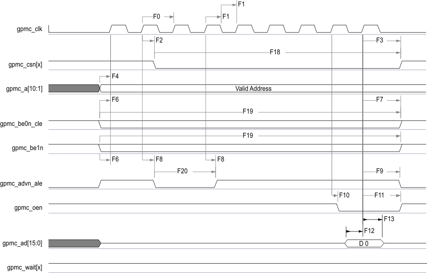
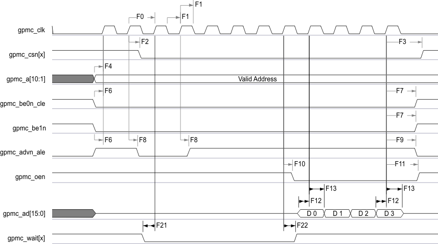
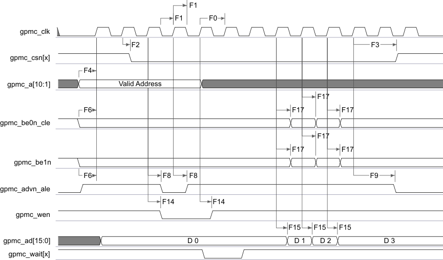
7.7.1.1 GPMC and NOR Flash—Synchronous Mode
Table 7-21 and Table 7-22 assume testing over the recommended operating conditions and electrical characteristic conditions shown in Table 7-20 (see Figure 7-17 through Figure 7-21).
Table 7-20 GPMC and NOR Flash Timing Conditions—Synchronous Mode
| PARAMETER | MIN | TYP | MAX | UNIT | |
|---|---|---|---|---|---|
| Input Conditions | |||||
| tR | Input signal rise time | 1 | 5 | ns | |
| tF | Input signal fall time | 1 | 5 | ns | |
| Output Condition | |||||
| CLOAD | Output load capacitance | 3 | 30 | pF | |
Table 7-21 GPMC and NOR Flash Timing Requirements—Synchronous Mode
| NO. | OPP100 | OPP50 | UNIT | |||||
|---|---|---|---|---|---|---|---|---|
| MIN | MAX | MIN | MAX | |||||
| F12 | tsu(dV-clkH) | Setup time, input data gpmc_ad[15:0] valid before output clock gpmc_clk high | 3.2 | 13.2 | ns | |||
| F13 | th(clkH-dV) | Hold time, input data gpmc_ad[15:0] valid after output clock gpmc_clk high | Industrial extended temperature (-40°C to 125°C) |
4.74 | 4.74 | ns | ||
| All other temperature ranges | 4.74 | 2.75 | ||||||
| F21 | tsu(waitV-clkH) | Setup time, input wait gpmc_wait[x](1) valid before output clock gpmc_clk high | 3.2 | 13.2 | ns | |||
| F22 | th(clkH-waitV) | Hold time, input wait gpmc_wait[x](1) valid after output clock gpmc_clk high | Industrial extended temperature (-40°C to 125°C) |
4.74 | 4.74 | ns | ||
| All other temperature ranges | 4.74 | 2.75 | ||||||
- In gpmc_wait[x], x is equal to 0 or 1.
Table 7-22 GPMC and NOR Flash Switching Characteristics—Synchronous Mode(2)
| NO. | PARAMETER | OPP100 | OPP50 | UNIT | ||||
|---|---|---|---|---|---|---|---|---|
| MIN | MAX | MIN | MAX | |||||
| F0 | 1 / tc(clk) | Frequency(18), output clock gpmc_clk | 100 | 50 | MHz | |||
| F1 | tw(clkH) | Typical pulse duration, output clock gpmc_clk high | 0.5P(15) | 0.5P(15) | 0.5P(15) | 0.5P(15) | ns | |
| F1 | tw(clkL) | Typical pulse duration, output clock gpmc_clk low | 0.5P(15) | 0.5P(15) | 0.5P(15) | 0.5P(15) | ns | |
| tdc(clk) | Duty cycle error, output clock gpmc_clk | –500 | 500 | –500 | 500 | ps | ||
| tJ(clk) | Jitter standard deviation(19), output clock gpmc_clk | 33.33 | 33.33 | ps | ||||
| tR(clk) | Rise time, output clock gpmc_clk | 2 | 2 | ns | ||||
| tF(clk) | Fall time, output clock gpmc_clk | 2 | 2 | ns | ||||
| tR(do) | Rise time, output data gpmc_ad[15:0] | 2 | 2 | ns | ||||
| tF(do) | Fall time, output data gpmc_ad[15:0] | 2 | 2 | ns | ||||
| F2 | td(clkH-csnV) | Delay time, output clock gpmc_clk rising edge to output chip select gpmc_csn[x](14) transition | F(6) - 2.2 | F(6) + 4.5 | F(6) - 3.2 | F(6) + 9.5 | ns | |
| F3 | td(clkH-csnIV) | Delay time, output clock gpmc_clk rising edge to output chip select gpmc_csn[x](14) invalid | E(5) – 2.2 | E(5) + 4.5 | E(5) – 3.2 | E(5) + 9.5 | ns | |
| F4 | td(aV-clk) | Delay time, output address gpmc_a[27:1] valid to output clock gpmc_clk first edge | B(2) – 4.5 | B(2) + 2.3 | B(2) – 5.5 | B(2) + 12.3 | ns | |
| F5 | td(clkH-aIV) | Delay time, output clock gpmc_clk rising edge to output address gpmc_a[27:1] invalid | –2.3 | 4.5 | –3.3 | 14.5 | ns | |
| F6 | td(be[x]nV-clk) | Delay time, output lower byte enable and command latch enable gpmc_be0n_cle, output upper byte enable gpmc_be1n valid to output clock gpmc_clk first edge | B(2) – 1.9 | B(2) + 2.3 | B(2) – 2.9 | B(2) + 12.3 | ns | |
| F7 | td(clkH-be[x]nIV) | Delay time, output clock gpmc_clk rising edge to output lower byte enable and command latch enable gpmc_be0n_cle, output upper byte enable gpmc_be1n invalid(11) | D(4) – 2.3 | D(4) + 1.9 | D(4) – 3.3 | D(4) + 6.9 | ns | |
| F7 | td(clkL-be[x]nIV) | Delay time, gpmc_clk falling edge to gpmc_nbe0_cle, gpmc_nbe1 invalid(12) | D(4) – 2.3 | D(4) + 1.9 | D(4) – 3.3 | D(4) + 6.9 | ns | |
| F7 | td(clkL-be[x]nIV) | Delay time, gpmc_clk falling edge to gpmc_nbe0_cle, gpmc_nbe1 invalid(13) | D(4) – 2.3 | D(4) + 1.9 | D(4) – 3.3 | D(4) + 11.9 | ns | |
| F8 | td(clkH-advn) | Delay time, output clock gpmc_clk rising edge to output address valid and address latch enable gpmc_advn_ale transition | G(7) – 2.3 | G(7) + 4.5 | G(7) – 3.3 | G(7) + 9.5 | ns | |
| F9 | td(clkH-advnIV) | Delay time, output clock gpmc_clk rising edge to output address valid and address latch enable gpmc_advn_ale invalid | D(4) – 2.3 | D(4) + 3.5 | D(4) – 3.3 | D(4) + 9.5 | ns | |
| F10 | td(clkH-oen) | Delay time, output clock gpmc_clk rising edge to output enable gpmc_oen transition | H(8) – 2.3 | H(8) + 3.5 | H(8) – 3.3 | H(8) + 8.5 | ns | |
| F11 | td(clkH-oenIV) | Delay time, output clock gpmc_clk rising edge to output enable gpmc_oen invalid | E(8) – 2.3 | E(8) + 3.5 | E(8) – 3.3 | E(8) + 8.5 | ns | |
| F14 | td(clkH-wen) | Delay time, output clock gpmc_clk rising edge to output write enable gpmc_wen transition | I(9) – 2.3 | I(9) + 4.5 | I(9) – 3.3 | I(9) + 9.5 | ns | |
| F15 | td(clkH-do) | Delay time, output clock gpmc_clk rising edge to output data gpmc_ad[15:0] transition(11) | J(10) – 2.3 | J(10) + 1.9 | J(10) – 3.3 | J(10) + 6.9 | ns | |
| F15 | td(clkL-do) | Delay time, gpmc_clk falling edge to gpmc_ad[15:0] data bus transition(12) | J(10) – 2.3 | J(10) + 1.9 | J(10) – 3.3 | J(10) + 6.9 | ns | |
| F15 | td(clkL-do) | Delay time, gpmc_clk falling edge to gpmc_ad[15:0] data bus transition(13) | J(10) – 2.3 | J(10) + 1.9 | J(10) – 3.3 | J(10) + 11.9 | ns | |
| F17 | td(clkH-be[x]n) | Delay time, output clock gpmc_clk rising edge to output lower byte enable and command latch enable gpmc_be0n_cle transition(11) | J(10) – 2.3 | J(10) + 1.9 | J(10) – 3.3 | J(10) + 6.9 | ns | |
| F17 | td(clkL-be[x]n) | Delay time, gpmc_clk falling edge to gpmc_nbe0_cle, gpmc_nbe1 transition(12) | J(10) – 2.3 | J(10) + 1.9 | J(10) – 3.3 | J(10) + 6.9 | ns | |
| F17 | td(clkL-be[x]n) | Delay time, gpmc_clk falling edge to gpmc_nbe0_cle, gpmc_nbe1 transition(13) | J(10) – 2.3 | J(10) + 1.9 | J(10) – 3.3 | J(10) + 11.9 | ns | |
| F18 | tw(csnV) | Pulse duration, output chip select gpmc_csn[x](14) low | Read | A(1) | A(1) | ns | ||
| Write | A(1) | A(1) | ns | |||||
| F19 | tw(be[x]nV) | Pulse duration, output lower byte enable and command latch enable gpmc_be0n_cle, output upper byte enable gpmc_be1n low | Read | C(3) | C(3) | ns | ||
| Write | C(3) | C(3) | ns | |||||
| F20 | tw(advnV) | Pulse duration, output address valid and address latch enable gpmc_advn_ale low | Read | K(16) | K(16) | ns | ||
| Write | K(16) | K(16) | ns | |||||
- For single read: A = (CSRdOffTime – CSOnTime) × (TimeParaGranularity + 1) × GPMC_FCLK(17)
For burst read: A = (CSRdOffTime – CSOnTime + (n – 1) × PageBurstAccessTime) × (TimeParaGranularity + 1) × GPMC_FCLK(17)
For burst write: A = (CSWrOffTime – CSOnTime + (n – 1) × PageBurstAccessTime) × (TimeParaGranularity + 1) × GPMC_FCLK(17)
With n being the page burst access number. - B = ClkActivationTime × GPMC_FCLK(17)
- For single read: C = RdCycleTime × (TimeParaGranularity + 1) × GPMC_FCLK (17)
For burst read: C = (RdCycleTime + (n – 1) × PageBurstAccessTime) × (TimeParaGranularity + 1) × GPMC_FCLK(17)
For burst write: C = (WrCycleTime + (n – 1) × PageBurstAccessTime) × (TimeParaGranularity + 1) × GPMC_FCLK(17)
With n being the page burst access number. - For single read: D = (RdCycleTime – AccessTime) × (TimeParaGranularity + 1) × GPMC_FCLK(17)
For burst read: D = (RdCycleTime – AccessTime) × (TimeParaGranularity + 1) × GPMC_FCLK(17)
For burst write: D = (WrCycleTime – AccessTime) × (TimeParaGranularity + 1) × GPMC_FCLK(17) - For single read: E = (CSRdOffTime – AccessTime) × (TimeParaGranularity + 1) × GPMC_FCLK(17)
For burst read: E = (CSRdOffTime – AccessTime) × (TimeParaGranularity + 1) × GPMC_FCLK(17)
For burst write: E = (CSWrOffTime – AccessTime) × (TimeParaGranularity + 1) × GPMC_FCLK(17) - For csn falling edge (CS activated):
- Case GpmcFCLKDivider = 0:
- F = 0.5 × CSExtraDelay × GPMC_FCLK(17)
- Case GpmcFCLKDivider = 1:
- Case GpmcFCLKDivider = 2:
- F = 0.5 × CSExtraDelay × GPMC_FCLK(17) if ((CSOnTime – ClkActivationTime) is a multiple of 3)
- F = (1 + 0.5 × CSExtraDelay) × GPMC_FCLK(17) if ((CSOnTime – ClkActivationTime – 1) is a multiple of 3)
- F = (2 + 0.5 × CSExtraDelay) × GPMC_FCLK(17) if ((CSOnTime – ClkActivationTime – 2) is a multiple of 3)
- Case GpmcFCLKDivider = 0:
- For ADV falling edge (ADV activated):
- Case GpmcFCLKDivider = 0:
- G = 0.5 × ADVExtraDelay × GPMC_FCLK(17)
- Case GpmcFCLKDivider = 1:
- Case GpmcFCLKDivider = 2:
- G = 0.5 × ADVExtraDelay × GPMC_FCLK(17) if ((ADVOnTime – ClkActivationTime) is a multiple of 3)
- G = (1 + 0.5 × ADVExtraDelay) × GPMC_FCLK(17) if ((ADVOnTime – ClkActivationTime – 1) is a multiple of 3)
- G = (2 + 0.5 × ADVExtraDelay) × GPMC_FCLK(17) if ((ADVOnTime – ClkActivationTime – 2) is a multiple of 3)
For ADV rising edge (ADV deactivated) in Reading mode:- Case GpmcFCLKDivider = 0:
- G = 0.5 × ADVExtraDelay × GPMC_FCLK(17)
- Case GpmcFCLKDivider = 1:
- Case GpmcFCLKDivider = 2:
- G = 0.5 × ADVExtraDelay × GPMC_FCLK(17) if ((ADVRdOffTime – ClkActivationTime) is a multiple of 3)
- G = (1 + 0.5 × ADVExtraDelay) × GPMC_FCLK(17) if ((ADVRdOffTime – ClkActivationTime – 1) is a multiple of 3)
- G = (2 + 0.5 × ADVExtraDelay) × GPMC_FCLK(17) if ((ADVRdOffTime – ClkActivationTime – 2) is a multiple of 3)
For ADV rising edge (ADV deactivated) in Writing mode:- Case GpmcFCLKDivider = 0:
- G = 0.5 × ADVExtraDelay × GPMC_FCLK(17)
- Case GpmcFCLKDivider = 1:
- Case GpmcFCLKDivider = 2:
- G = 0.5 × ADVExtraDelay × GPMC_FCLK(17) if ((ADVWrOffTime – ClkActivationTime) is a multiple of 3)
- G = (1 + 0.5 × ADVExtraDelay) × GPMC_FCLK(17) if ((ADVWrOffTime – ClkActivationTime – 1) is a multiple of 3)
- G = (2 + 0.5 × ADVExtraDelay) × GPMC_FCLK(17) if ((ADVWrOffTime – ClkActivationTime – 2) is a multiple of 3)
- Case GpmcFCLKDivider = 0:
- For OE falling edge (OE activated) and I/O DIR rising edge (Data Bus input direction):
- Case GpmcFCLKDivider = 0:
- H = 0.5 × OEExtraDelay × GPMC_FCLK(17)
- Case GpmcFCLKDivider = 1:
- Case GpmcFCLKDivider = 2:
- H = 0.5 × OEExtraDelay × GPMC_FCLK(17) if ((OEOnTime – ClkActivationTime) is a multiple of 3)
- H = (1 + 0.5 × OEExtraDelay) × GPMC_FCLK(17) if ((OEOnTime – ClkActivationTime – 1) is a multiple of 3)
- H = (2 + 0.5 × OEExtraDelay) × GPMC_FCLK(17) if ((OEOnTime – ClkActivationTime – 2) is a multiple of 3)
For OE rising edge (OE deactivated):- Case GpmcFCLKDivider = 0:
- H = 0.5 × OEExtraDelay × GPMC_FCLK(17)
- Case GpmcFCLKDivider = 1:
- Case GpmcFCLKDivider = 2:
- H = 0.5 × OEExtraDelay × GPMC_FCLK(17) if ((OEOffTime – ClkActivationTime) is a multiple of 3)
- H = (1 + 0.5 × OEExtraDelay) × GPMC_FCLK(17) if ((OEOffTime – ClkActivationTime – 1) is a multiple of 3)
- H = (2 + 0.5 × OEExtraDelay) × GPMC_FCLK(17) if ((OEOffTime – ClkActivationTime – 2) is a multiple of 3)
- Case GpmcFCLKDivider = 0:
- For WE falling edge (WE activated):
- Case GpmcFCLKDivider = 0:
- I = 0.5 × WEExtraDelay × GPMC_FCLK(17)
- Case GpmcFCLKDivider = 1:
- Case GpmcFCLKDivider = 2:
- I = 0.5 × WEExtraDelay × GPMC_FCLK(17) if ((WEOnTime – ClkActivationTime) is a multiple of 3)
- I = (1 + 0.5 × WEExtraDelay) × GPMC_FCLK(17) if ((WEOnTime – ClkActivationTime – 1) is a multiple of 3)
- I = (2 + 0.5 × WEExtraDelay) × GPMC_FCLK(17) if ((WEOnTime – ClkActivationTime – 2) is a multiple of 3)
For WE rising edge (WE deactivated):- Case GpmcFCLKDivider = 0:
- I = 0.5 × WEExtraDelay × GPMC_FCLK (17)
- Case GpmcFCLKDivider = 1:
- Case GpmcFCLKDivider = 2:
- I = 0.5 × WEExtraDelay × GPMC_FCLK(17) if ((WEOffTime – ClkActivationTime) is a multiple of 3)
- I = (1 + 0.5 × WEExtraDelay) × GPMC_FCLK(17) if ((WEOffTime – ClkActivationTime – 1) is a multiple of 3)
- I = (2 + 0.5 × WEExtraDelay) × GPMC_FCLK(17) if ((WEOffTime – ClkActivationTime – 2) is a multiple of 3)
- Case GpmcFCLKDivider = 0:
- J = GPMC_FCLK(17)
- First transfer only for CLK DIV 1 mode.
- Half cycle; for all data after initial transfer for CLK DIV 1 mode.
- Half cycle of GPMC_CLK_OUT; for all data for modes other than CLK DIV 1 mode. GPMC_CLK_OUT divide down from GPMC_FCLK.
- In gpmc_csn[x], x is equal to 0, 1, 2, 3, 4, or 5. In gpmc_wait[x], x is equal to 0 or 1.
- P = gpmc_clk period in ns
- For read: K = (ADVRdOffTime – ADVOnTime) × (TimeParaGranularity + 1) × GPMC_FCLK(17)
For write: K = (ADVWrOffTime – ADVOnTime) × (TimeParaGranularity + 1) × GPMC_FCLK(17) - GPMC_FCLK is general-purpose memory controller internal functional clock period in ns.
- Related to the gpmc_clk output clock maximum and minimum frequencies programmable in the GPMC module by setting the GPMC_CONFIG1_CSx configuration register bit field GpmcFCLKDivider.
- The jitter probability density can be approximated by a Gaussian function.
7.7.1.2 GPMC and NOR Flash—Asynchronous Mode
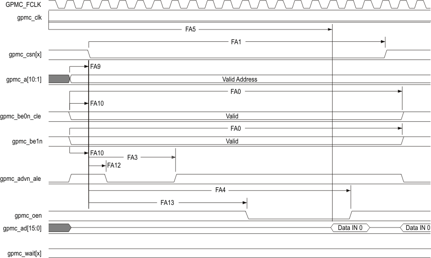
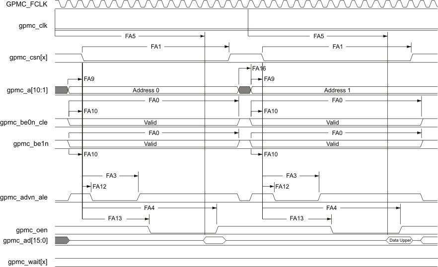
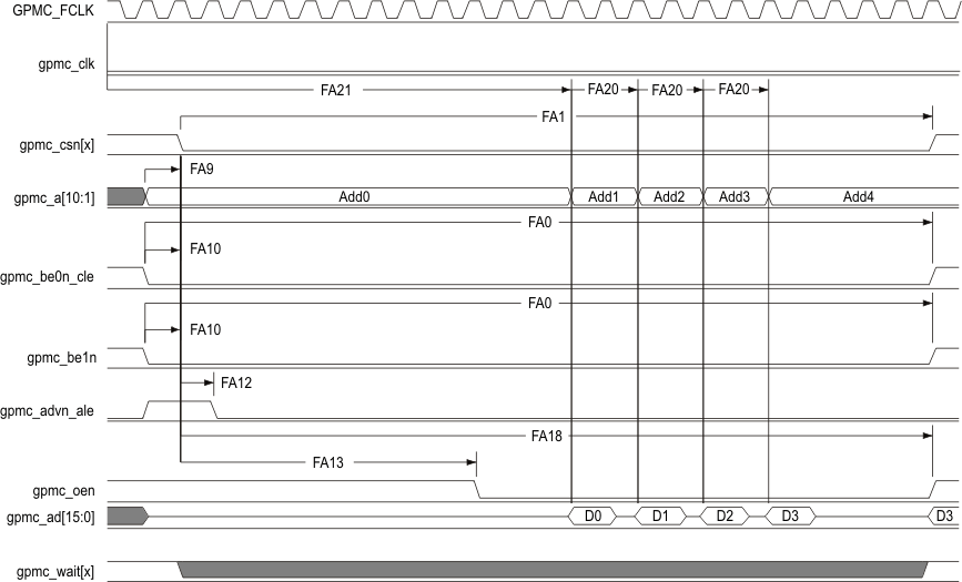
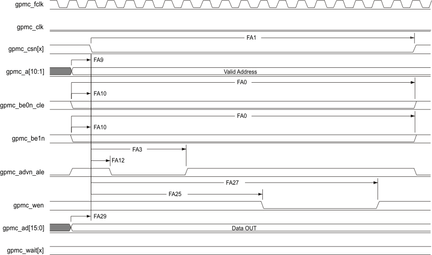
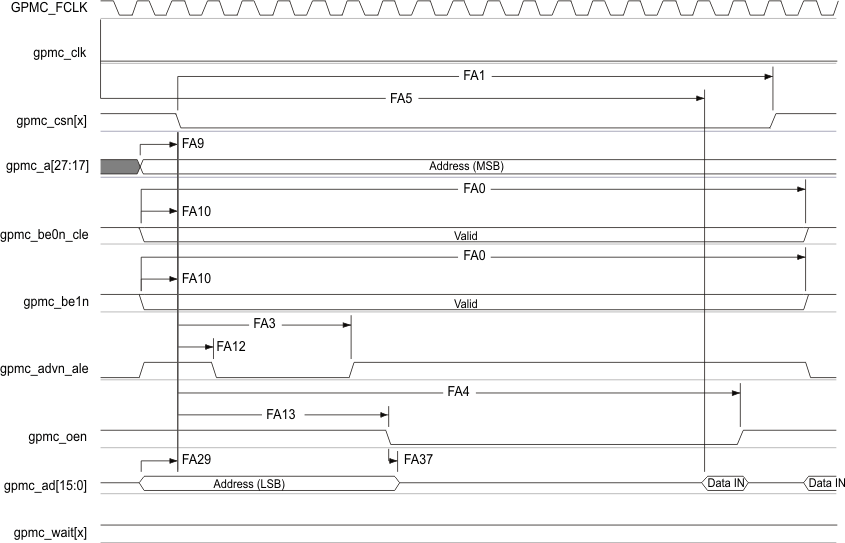
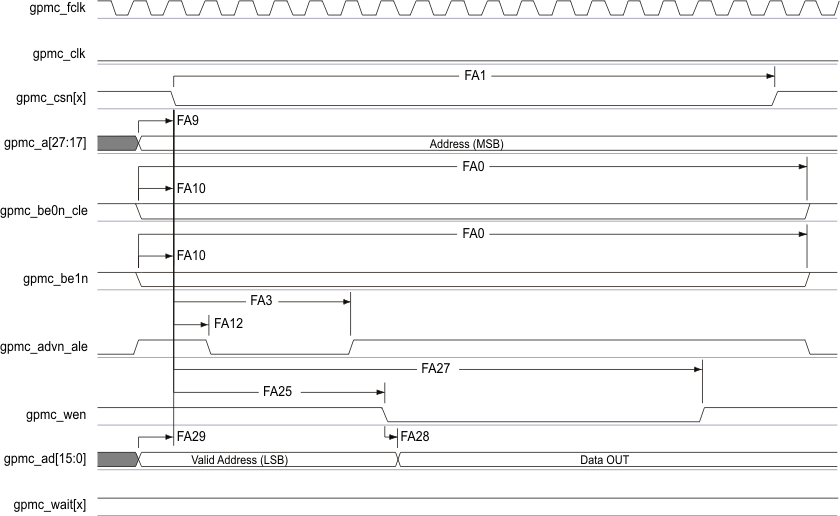
Table 7-24 and Table 7-25 assume testing over the recommended operating conditions and electrical characteristic conditions shown in Table 7-23 (see Figure 7-22 through Figure 7-27).
Table 7-23 GPMC and NOR Flash Timing Conditions—Asynchronous Mode
| MIN | TYP | MAX | UNIT | ||
|---|---|---|---|---|---|
| Input Conditions | |||||
| tR | Input signal rise time | 1 | 5 | ns | |
| tF | Input signal fall time | 1 | 5 | ns | |
| Output Condition | |||||
| CLOAD | Output load capacitance | 3 | 30 | pF | |
Table 7-24 GPMC and NOR Flash Internal Timing Requirements—Asynchronous Mode(1)(2)
| NO. | OPP100 | OPP50 | UNIT | |||
|---|---|---|---|---|---|---|
| MIN | MAX | MIN | MAX | |||
| FI1 | Delay time, output data gpmc_ad[15:0] generation from internal functional clock GPMC_FCLK(3) | 6.5 | 6.5 | ns | ||
| FI2 | Delay time, input data gpmc_ad[15:0] capture from internal functional clock GPMC_FCLK(3) | 4 | 4 | ns | ||
| FI3 | Delay time, output chip select gpmc_csn[x] generation from internal functional clock GPMC_FCLK(3) | 6.5 | 6.5 | ns | ||
| FI4 | Delay time, output address gpmc_a[27:1] generation from internal functional clock GPMC_FCLK(3) | 6.5 | 6.5 | ns | ||
| FI5 | Delay time, output address gpmc_a[27:1] valid from internal functional clock GPMC_FCLK(3) | 6.5 | 6.5 | ns | ||
| FI6 | Delay time, output lower-byte enable and command latch enable gpmc_be0n_cle, output upper-byte enable gpmc_be1n generation from internal functional clock GPMC_FCLK(3) | 6.5 | 6.5 | ns | ||
| FI7 | Delay time, output enable gpmc_oen generation from internal functional clock GPMC_FCLK(3) | 6.5 | 6.5 | ns | ||
| FI8 | Delay time, output write enable gpmc_wen generation from internal functional clock GPMC_FCLK(3) | 6.5 | 6.5 | ns | ||
| FI9 | Skew, internal functional clock GPMC_FCLK(3) | 100 | 100 | ps | ||
- The internal parameters table must be used to calculate data access time stored in the corresponding CS register bit field.
- Internal parameters are referred to the GPMC functional internal clock which is not provided externally.
- GPMC_FCLK is general-purpose memory controller internal functional clock.
Table 7-25 GPMC and NOR Flash Timing Requirements—Asynchronous Mode
| NO. | OPP100 | OPP50 | UNIT | ||||
|---|---|---|---|---|---|---|---|
| MIN | MAX | MIN | MAX | ||||
| FA5(1) | tacc(d) | Data access time | H(5) | H(5) | ns | ||
| FA20(2) | tacc1-pgmode(d) | Page mode successive data access time | P(4) | P(4) | ns | ||
| FA21(3) | tacc2-pgmode(d) | Page mode first data access time | H(5) | H(5) | ns | ||
- The FA5 parameter shows the amount of time required to internally sample input data. It is expressed in number of GPMC functional clock cycles. From start of read cycle and after FA5 functional clock cycles, input data is internally sampled by active functional clock edge. FA5 value must be stored inside the AccessTime register bit field.
- The FA20 parameter shows amount of time required to internally sample successive input page data. It is expressed in number of GPMC functional clock cycles. After each access to input page data, next input page data is internally sampled by active functional clock edge after FA20 functional clock cycles. The FA20 value must be stored in the PageBurstAccessTime register bit field.
- The FA21 parameter shows amount of time required to internally sample first input page data. It is expressed in number of GPMC functional clock cycles. From start of read cycle and after FA21 functional clock cycles, first input page data is internally sampled by active functional clock edge. FA21 value must be stored inside the AccessTime register bit field.
- P = PageBurstAccessTime × (TimeParaGranularity + 1) × GPMC_FCLK(6)
- H = AccessTime × (TimeParaGranularity + 1) × GPMC_FCLK(6)
- GPMC_FCLK is general-purpose memory controller internal functional clock period in ns.
Table 7-26 GPMC and NOR Flash Switching Characteristics—Asynchronous Mode
| NO. | PARAMETER | OPP100 | OPP50 | UNIT | ||||
|---|---|---|---|---|---|---|---|---|
| MIN | MAX | MIN | MAX | |||||
| tR(d) | Rise time, output data gpmc_ad[15:0] | 2 | 2 | ns | ||||
| tF(d) | Fall time, output data gpmc_ad[15:0] | 2 | 2 | ns | ||||
| FA0 | tw(be[x]nV) | Pulse duration, output lower-byte enable and command latch enable gpmc_be0n_cle, output upper-byte enable gpmc_be1n valid time | Read | N(12) | N(12) | ns | ||
| Write | N(12) | N(12) | ||||||
| FA1 | tw(csnV) | Pulse duration, output chip select gpmc_csn[x](13) low | Read | A(1) | A(1) | ns | ||
| Write | A(1) | A(1) | ||||||
| FA3 | td(csnV-advnIV) | Delay time, output chip select gpmc_csn[x](13) valid to output address valid and address latch enable gpmc_advn_ale invalid | Read | B(2) – 0.2 | B(2) + 2.0 | B(2) – 5 | B(2) + 5 | ns |
| Write | B(2) – 0.2 | B(2) + 2.0 | B(2) – 5 | B(2) + 5 | ||||
| FA4 | td(csnV-oenIV) | Delay time, output chip select gpmc_csn[x](13) valid to output enable gpmc_oen invalid (Single read) | C(3) – 0.2 | C(3) + 2.0 | C(3) – 5 | C(3) + 5 | ns | |
| FA9 | td(aV-csnV) | Delay time, output address gpmc_a[27:1] valid to output chip select gpmc_csn[x](13) valid | J(9) – 0.2 | J(9) + 2.0 | J(9) – 5 | J(9) + 5 | ns | |
| FA10 | td(be[x]nV-csnV) | Delay time, output lower-byte enable and command latch enable gpmc_be0n_cle, output upper-byte enable gpmc_be1n valid to output chip select gpmc_csn[x](13) valid | J(9) – 0.2 | J(9) + 2.0 | J(9) – 5 | J(9) + 5 | ns | |
| FA12 | td(csnV-advnV) | Delay time, output chip select gpmc_csn[x](13) valid to output address valid and address latch enable gpmc_advn_ale valid | K(10) – 0.2 | K(10) + 2.0 | K(10) – 5 | K(10) + 5 | ns | |
| FA13 | td(csnV-oenV) | Delay time, output chip select gpmc_csn[x](13) valid to output enable gpmc_oen valid | L(11) – 0.2 | L(11) + 2.0 | L (11) – 5 | L(11) + 5 | ns | |
| FA16 | tw(aIV) | Pulse durationm output address gpmc_a[26:1] invalid between 2 successive read and write accesses | G(7) | G(7) | ns | |||
| FA18 | td(csnV-oenIV) | Delay time, output chip select gpmc_csn[x](13) valid to output enable gpmc_oen invalid (Burst read) | I(8) – 0.2 | I(8) + 2.0 | I(8) – 5 | I(8) + 5 | ns | |
| FA20 | tw(aV) | Pulse duration, output address gpmc_a[27:1] valid - 2nd, 3rd, and 4th accesses | D(4) | D(4) | ns | |||
| FA25 | td(csnV-wenV) | Delay time, output chip select gpmc_csn[x](13) valid to output write enable gpmc_wen valid | E(5) – 0.2 | E(5) + 2.0 | E(5) – 5 | E(5) + 5 | ns | |
| FA27 | td(csnV-wenIV) | Delay time, output chip select gpmc_csn[x](13) valid to output write enable gpmc_wen invalid | F(6) – 0.2 | F(6) + 2.0 | F(6) – 5 | F(6) + 5 | ns | |
| FA28 | td(wenV-dV) | Delay time, output write enable gpmc_ wen valid to output data gpmc_ad[15:0] valid | 2.0 | 5 | ns | |||
| FA29 | td(dV-csnV) | Delay time, output data gpmc_ad[15:0] valid to output chip select gpmc_csn[x](13) valid | J(9) – 0.2 | J(9) + 2.0 | J(9) – 5 | J(9) + 5 | ns | |
| FA37 | td(oenV-aIV) | Delay time, output enable gpmc_oen valid to output address gpmc_ad[15:0] phase end | 2.0 | 5 | ns | |||
- For single read: A = (CSRdOffTime – CSOnTime) × (TimeParaGranularity + 1) × GPMC_FCLK(14)
For single write: A = (CSWrOffTime – CSOnTime) × (TimeParaGranularity + 1) × GPMC_FCLK(14)
For burst read: A = (CSRdOffTime – CSOnTime + (n – 1) × PageBurstAccessTime) × (TimeParaGranularity + 1) × GPMC_FCLK(14)
For burst write: A = (CSWrOffTime – CSOnTime + (n – 1) × PageBurstAccessTime) × (TimeParaGranularity + 1) × GPMC_FCLK(14)
with n being the page burst access number - For reading: B = ((ADVRdOffTime – CSOnTime) × (TimeParaGranularity + 1) + 0.5 × (ADVExtraDelay – CSExtraDelay)) × GPMC_FCLK(14)
For writing: B = ((ADVWrOffTime – CSOnTime) × (TimeParaGranularity + 1) + 0.5 × (ADVExtraDelay – CSExtraDelay)) × GPMC_FCLK(14) - C = ((OEOffTime – CSOnTime) × (TimeParaGranularity + 1) + 0.5 × (OEExtraDelay – CSExtraDelay)) × GPMC_FCLK(14)
- D = PageBurstAccessTime × (TimeParaGranularity + 1) × GPMC_FCLK(14)
- E = ((WEOnTime – CSOnTime) × (TimeParaGranularity + 1) + 0.5 × (WEExtraDelay – CSExtraDelay)) × GPMC_FCLK(14)
- F = ((WEOffTime – CSOnTime) × (TimeParaGranularity + 1) + 0.5 × (WEExtraDelay – CSExtraDelay)) × GPMC_FCLK(14)
- G = Cycle2CycleDelay × GPMC_FCLK(14)
- I = ((OEOffTime + (n – 1) × PageBurstAccessTime – CSOnTime) × (TimeParaGranularity + 1) + 0.5 × (OEExtraDelay – CSExtraDelay)) × GPMC_FCLK(14)
- J = (CSOnTime × (TimeParaGranularity + 1) + 0.5 × CSExtraDelay) × GPMC_FCLK(14)
- K = ((ADVOnTime – CSOnTime) × (TimeParaGranularity + 1) + 0.5 × (ADVExtraDelay – CSExtraDelay)) × GPMC_FCLK(14)
- L = ((OEOnTime – CSOnTime) × (TimeParaGranularity + 1) + 0.5 × (OEExtraDelay – CSExtraDelay)) × GPMC_FCLK(14)
- For single read: N = RdCycleTime × (TimeParaGranularity + 1) × GPMC_FCLK(14)
For single write: N = WrCycleTime × (TimeParaGranularity + 1) × GPMC_FCLK(14)
For burst read: N = (RdCycleTime + (n – 1) × PageBurstAccessTime) × (TimeParaGranularity + 1) × GPMC_FCLK(14)
For burst write: N = (WrCycleTime + (n – 1) × PageBurstAccessTime) × (TimeParaGranularity + 1) × GPMC_FCLK(14) - In gpmc_csn[x], x is equal to 0, 1, 2, 3, 4, or 5.
- GPMC_FCLK is general-purpose memory controller internal functional clock period in ns.
7.7.1.3 GPMC and NAND Flash—Asynchronous Mode
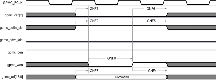
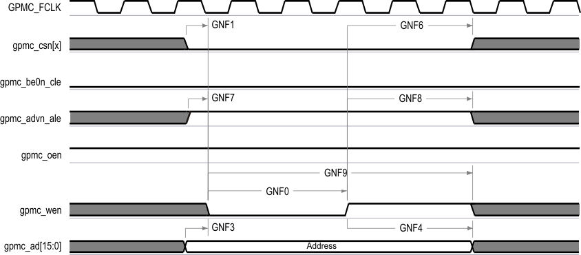
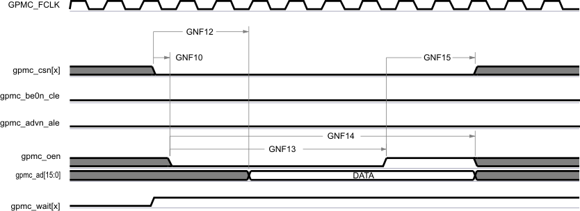
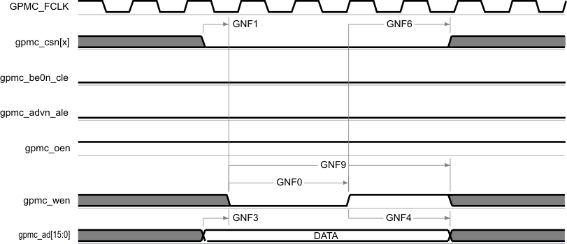
Table 7-28 and Table 7-29 assume testing over the recommended operating conditions and electrical characteristic conditions shown in Table 7-27 (see Figure 7-28 through Figure 7-31).
Table 7-27 GPMC and NAND Flash Timing Conditions—Asynchronous Mode
| PARAMETER | MIN | TYP | MAX | UNIT | |
|---|---|---|---|---|---|
| Input Conditions | |||||
| tR | Input signal rise time | 1 | 5 | ns | |
| tF | Input signal fall time | 1 | 5 | ns | |
| Output Condition | |||||
| CLOAD | Output load capacitance | 3 | 30 | pF | |
Table 7-28 GPMC and NAND Flash Internal Timing Requirements—Asynchronous Mode(1)(2)
| NO. | OPP100 | OPP50 | UNIT | |||
|---|---|---|---|---|---|---|
| MIN | MAX | MIN | MAX | |||
| GNFI1 | Delay time, output data gpmc_ad[15:0] generation from internal functional clock GPMC_FCLK(3) | 6.5 | 6.5 | ns | ||
| GNFI2 | Delay time, input data gpmc_ad[15:0] capture from internal functional clock GPMC_FCLK(3) | 4.0 | 4.0 | ns | ||
| GNFI3 | Delay time, output chip select gpmc_csn[x] generation from internal functional clock GPMC_FCLK(3) | 6.5 | 6.5 | ns | ||
| GNFI4 | Delay time, output address valid and address latch enable gpmc_advn_ale generation from internal functional clock GPMC_FCLK(3) | 6.5 | 6.5 | ns | ||
| GNFI5 | Delay time, output lower-byte enable and command latch enable gpmc_be0n_cle generation from internal functional clock GPMC_FCLK(3) | 6.5 | 6.5 | ns | ||
| GNFI6 | Delay time, output enable gpmc_oen generation from internal functional clock GPMC_FCLK(3) | 6.5 | 6.5 | ns | ||
| GNFI7 | Delay time, output write enable gpmc_wen generation from internal functional clock GPMC_FCLK(3) | 6.5 | 6.5 | ns | ||
| GNFI8 | Skew, functional clock GPMC_FCLK(3) | 100 | 100 | ps | ||
- Internal parameters table must be used to calculate data access time stored in the corresponding CS register bit field.
- Internal parameters are referred to the GPMC functional internal clock which is not provided externally.
- GPMC_FCLK is general-purpose memory controller internal functional clock.
Table 7-29 GPMC and NAND Flash Timing Requirements—Asynchronous Mode
| NO. | OPP100 | OPP50 | UNIT | ||||
|---|---|---|---|---|---|---|---|
| MIN | MAX | MIN | MAX | ||||
| GNF12(1) | tacc(d) | Access time, input data gpmc_ad[15:0] | J(2) | J(2) | ns | ||
- The GNF12 parameter illustrates the amount of time required to internally sample input data. It is expressed in number of GPMC functional clock cycles. From start of the read cycle and after GNF12 functional clock cycles, input data is internally sampled by the active functional clock edge. The GNF12 value must be stored inside AccessTime register bit field.
- J = AccessTime × (TimeParaGranularity + 1) × GPMC_FCLK(3)
- GPMC_FCLK is general-purpose memory controller internal functional clock period in ns.
Table 7-30 GPMC and NAND Flash Switching Characteristics—Asynchronous Mode
| NO. | PARAMETER | OPP100 | OPP50 | UNIT | |||
|---|---|---|---|---|---|---|---|
| MIN | MAX | MIN | MAX | ||||
| tR(d) | Rise time, output data gpmc_ad[15:0] | 2 | 2 | ns | |||
| tF(d) | Fall time, output data gpmc_ad[15:0] | 2 | 2 | ns | |||
| GNF0 | tw(wenV) | Pulse duration, output write enable gpmc_wen valid | A(1) | A(1) | ns | ||
| GNF1 | td(csnV-wenV) | Delay time, output chip select gpmc_csn[x](13) valid to output write enable gpmc_wen valid | B(2) – 0.2 | B(2) + 2.0 | B(2) – 5 | B(2) + 5 | ns |
| GNF2 | tw(cleH-wenV) | Delay time, output lower-byte enable and command latch enable gpmc_be0n_cle high to output write enable gpmc_wen valid | C(3) – 0.2 | C(3) + 2.0 | C(3) – 5 | C(3) + 5 | ns |
| GNF3 | tw(wenV-dV) | Delay time, output data gpmc_ad[15:0] valid to output write enable gpmc_wen valid | D(4) – 0.2 | D(4) + 2.0 | D(4) – 5 | D(4) + 5 | ns |
| GNF4 | tw(wenIV-dIV) | Delay time, output write enable gpmc_wen invalid to output data gpmc_ad[15:0] invalid | E(5) – 0.2 | E(5) + 5 | E(5) – 5 | E(5) + 5 | ns |
| GNF5 | tw(wenIV-cleIV) | Delay time, output write enable gpmc_wen invalid to output lower-byte enable and command latch enable gpmc_be0n_cle invalid | F(6) – 0.2 | F(6) + 2.0 | F(6) – 5 | F(6) + 5 | ns |
| GNF6 | tw(wenIV-csnIV) | Delay time, output write enable gpmc_wen invalid to output chip select gpmc_csn[x](13) invalid | G(7) – 0.2 | G(7) + 2.0 | G(7) – 5 | G(7) + 5 | ns |
| GNF7 | tw(aleH-wenV) | Delay time, output address valid and address latch enable gpmc_advn_ale high to output write enable gpmc_wen valid | C(3) – 0.2 | C(3) + 2.0 | C(3) – 5 | C(3) + 5 | ns |
| GNF8 | tw(wenIV-aleIV) | Delay time, output write enable gpmc_wen invalid to output address valid and address latch enable gpmc_advn_ale invalid | F(6) – 0.2 | F(6) + 2.0 | F(6) – 5 | F(6) + 5 | ns |
| GNF9 | tc(wen) | Cycle time, write | H(8) | H(8) | ns | ||
| GNF10 | td(csnV-oenV) | Delay time, output chip select gpmc_csn[x](13) valid to output enable gpmc_oen valid | I(9) – 0.2 | I(9) + 2.0 | I(9) – 5 | I(9) + 5 | ns |
| GNF13 | tw(oenV) | Pulse duration, output enable gpmc_oen valid | K(10) | K(10) | ns | ||
| GNF14 | tc(oen) | Cycle time, read | L(11) | L(11) | ns | ||
| GNF15 | tw(oenIV-csnIV) | Delay time, output enable gpmc_oen invalid to output chip select gpmc_csn[x](13) invalid | M(12) – 0.2 | M(12) + 2.0 | M(12) – 5 | M(12) + 5 | ns |
- A = (WEOffTime – WEOnTime) × (TimeParaGranularity + 1) × GPMC_FCLK(14)
- B = ((WEOnTime – CSOnTime) × (TimeParaGranularity + 1) + 0.5 × (WEExtraDelay – CSExtraDelay)) × GPMC_FCLK(14)
- C = ((WEOnTime – ADVOnTime) × (TimeParaGranularity + 1) + 0.5 × (WEExtraDelay – ADVExtraDelay)) × GPMC_FCLK(14)
- D = (WEOnTime × (TimeParaGranularity + 1) + 0.5 × WEExtraDelay) × GPMC_FCLK(14)
- E = ((WrCycleTime – WEOffTime) × (TimeParaGranularity + 1) – 0.5 × WEExtraDelay) × GPMC_FCLK(14)
- F = ((ADVWrOffTime – WEOffTime) × (TimeParaGranularity + 1) + 0.5 × (ADVExtraDelay – WEExtraDelay)) × GPMC_FCLK(14)
- G = ((CSWrOffTime – WEOffTime) × (TimeParaGranularity + 1) + 0.5 × (CSExtraDelay – WEExtraDelay)) × GPMC_FCLK(14)
- H = WrCycleTime × (1 + TimeParaGranularity) × GPMC_FCLK(14)
- I = ((OEOnTime – CSOnTime) × (TimeParaGranularity + 1) + 0.5 × (OEExtraDelay – CSExtraDelay)) × GPMC_FCLK(14)
- K = (OEOffTime – OEOnTime) × (1 + TimeParaGranularity) × GPMC_FCLK(14)
- L = RdCycleTime × (1 + TimeParaGranularity) × GPMC_FCLK(14)
- M = ((CSRdOffTime – OEOffTime) × (TimeParaGranularity + 1) + 0.5 × (CSExtraDelay – OEExtraDelay)) × GPMC_FCLK(14)
- In gpmc_csn[x], x is equal to 0, 1, 2, 3, 4, or 5.
- GPMC_FCLK is general-purpose memory controller internal functional clock period in ns.
7.7.2 mDDR(LPDDR), DDR2, DDR3, DDR3L Memory Interface
The device has a dedicated interface to mDDR(LPDDR), DDR2, DDR3, and DDR3L SDRAM. It supports JEDEC standard compliant mDDR(LPDDR), DDR2, DDR3, and DDR3L SDRAM devices with a 16-bit data path to external SDRAM memory.
For more details on the mDDR(LPDDR), DDR2, DDR3, and DDR3L memory interface, see the EMIF section of the AM335x and AMIC110 Sitara Processors Technical Reference Manual.
7.7.2.1 mDDR (LPDDR) Routing Guidelines
It is common to find industry references to mobile double data rate (mDDR) when discussing JEDEC defined low-power double-data rate (LPDDR) memory devices. The following guidelines use LPDDR when referencing JEDEC defined low-power double-data rate memory devices.
7.7.2.1.1 Board Designs
TI only supports board designs that follow the guidelines outlined in this document. The switching characteristics and the timing diagram for the LPDDR memory interface are shown in Table 7-31 and Figure 7-32.
Table 7-31 Switching Characteristics for LPDDR Memory Interface
| NO. | PARAMETER | MIN | MAX | UNIT | |
|---|---|---|---|---|---|
| 1 | tc(DDR_CK)
tc(DDR_CKn) |
Cycle time, DDR_CK and DDR_CKn | 5 | (1) | ns |
- The JEDEC JESD209B specification only defines the maximum clock period for LPDDR333 and faster speed bin LPDDR memory devices. To determine the maximum clock period, see the respective LPDDR memory data sheet.
 Figure 7-32 LPDDR Memory Interface Clock Timing
7.7.2.1.2 LPDDR Interface
This section provides the timing specification for the LPDDR interface as a PCB design and manufacturing specification. The design rules constrain PCB trace length, PCB trace skew, signal integrity, cross-talk, and signal timing. These rules, when followed, result in a reliable LPDDR memory system without the need for a complex timing closure process. For more information regarding the guidelines for using this LPDDR specification, see Understanding TI’s PCB Routing Rule-Based DDR Timing Specification. This application report provides generic guidelines and approach. All the specifications provided in the data manual take precedence over the generic guidelines and must be adhered to for a reliable LPDDR interface operation.
7.7.2.1.2.1 LPDDR Interface Schematic
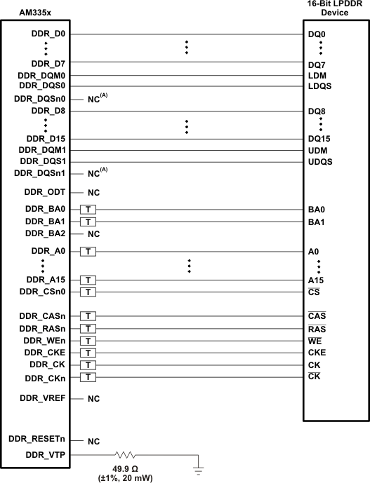
Figure 7-33 shows the schematic connections for 16-bit interface on the AM335x device using one x16 LPDDR device. The AM335x LPDDR memory interface only supports 16-bit-wide mode of operation. The AM335x device can only source one load connected to the DQS[x] and DQ[x] net class signals and one load connected to the CK and ADDR_CTRL net class signals. For more information related to net classes, see Section 7.7.2.1.2.8.
7.7.2.1.2.2 Compatible JEDEC LPDDR Devices
Table 7-32 shows the parameters of the JEDEC LPDDR devices that are compatible with this interface. Generally, the LPDDR interface is compatible with x16 LPDDR400 speed grade LPDDR devices.
Table 7-32 Compatible JEDEC LPDDR Devices (Per Interface)(1)
| NO. | PARAMETER | MIN | MAX | UNIT |
|---|---|---|---|---|
| 1 | JEDEC LPDDR device speed grade | LPDDR400 | ||
| 2 | JEDEC LPDDR device bit width | x16 | x16 | Bits |
| 3 | JEDEC LPDDR device count | 1 | Devices | |
| 4 | JEDEC LPDDR device terminal count | 60 | Terminals |
- If the LPDDR interface is operated with a clock frequency less than 200 MHz, lower-speed grade LPDDR devices may be used if the minimum clock period specified for the LPDDR device is less than or equal to the minimum clock period selected for the AM335x LPDDR interface.
7.7.2.1.2.3 PCB Stackup
The minimum stackup required for routing the AM335x device is a 4-layer stackup as shown in Table 7-33. Additional layers may be added to the PCB stackup to accommodate other circuitry, enhance signal integrity and electromagnetic interference performance, or to reduce the size of the PCB footprint.
Table 7-33 Minimum PCB Stackup(1)
| LAYER | TYPE | DESCRIPTION |
|---|---|---|
| 1 | Signal | Top signal routing |
| 2 | Plane | Ground |
| 3 | Plane | Split Power Plane |
| 4 | Signal | Bottom signal routing |
- All signals that have critical signal integrity requirements should be routed first on layer 1. It may not be possible to route all of these signals on layer 1, therefore requiring routing of some signals on layer 4. When this is done, the signal routes on layer 4 must not cross splits in the power plane.
Complete stackup specifications are provided in Table 7-34.
Table 7-34 PCB Stackup Specifications(1)
| NO. | PARAMETER | MIN | TYP | MAX | UNIT | |
|---|---|---|---|---|---|---|
| 1 | PCB routing and plane layers | 4 | ||||
| 2 | Signal routing layers | 2 | ||||
| 3 | Full ground layers under LPDDR routing region | 1 | ||||
| 4 | Number of ground plane cuts allowed within LPDDR routing region | 0 | ||||
| 5 | Full VDDS_DDR power reference layers under LPDDR routing region | 1 | ||||
| 6 | Number of layers between LPDDR routing layer and reference ground plane | 0 | ||||
| 7 | PCB routing feature size | 4 | mils | |||
| 8 | PCB trace width, w | 4 | mils | |||
| 9 | PCB BGA escape via pad size(2) | 18 | 20 | mils | ||
| 10 | PCB BGA escape via hole size(2) | 10 | mils | |||
| 11 | Single-ended impedance, Zo(3) | 50 | 75 | Ω | ||
| 12 | Impedance control(4)(5) | Zo-5 | Zo | Zo+5 | Ω | |
- For the LPDDR device BGA pad size, see the LPDDR device manufacturer documentation.
- A 20-10 via may be used if enough power routing resources are available. An 18-10 via allows for more flexible power routing to the AM335x device.
- Zo is the nominal singled-ended impedance selected for the PCB.
- This parameter specifies the AC characteristic impedance tolerance for each segment of a PCB signal trace relative to the chosen Zo defined by the single-ended impedance parameter.
- Tighter impedance control is required to ensure flight time skew is minimal.
7.7.2.1.2.4 Placement
Figure 7-34 shows the required placement for the LPDDR devices. The dimensions for this figure are defined in Table 7-35. The placement does not restrict the side of the PCB on which the devices are mounted. The ultimate purpose of the placement is to limit the maximum trace lengths and allow for proper routing space. For single-memory LPDDR systems, the second LPDDR device is omitted from the placement.
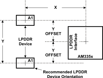 Figure 7-34 AM335x Device and LPDDR Device Placement
Table 7-35 Placement Specifications(1)
| NO. | PARAMETER | MIN | MAX | UNIT |
|---|---|---|---|---|
| 1 | X(2)(3) | 1750 | mils | |
| 2 | Y(2)(3) | 1280 | mils | |
| 3 | Y Offset(2)(3)(4) | 650 | mils | |
| 4 | Clearance from non-LPDDR signal to LPDDR keepout region(5)(6) | 4 | w |
- LPDDR keepout region to encompass entire LPDDR routing area.
- For dimension definitions, see Figure 7-34.
- Measurements from center of the AM335x device to center of LPDDR device.
- For single-memory systems, TI recommends that Y offset be as small as possible.
- w is defined as the signal trace width.
- Non-LPDDR signals allowed within LPDDR keepout region provided they are separated from LPDDR routing layers by a ground plane.
7.7.2.1.2.5 LPDDR Keepout Region
The region of the PCB used for the LPDDR circuitry must be isolated from other signals. The LPDDR keepout region is defined for this purpose and is shown in Figure 7-35. This region should encompass all LPDDR circuitry and the region size varies with component placement and LPDDR routing. Additional clearances required for the keepout region are shown in Table 7-35. Non-LPDDR signals must not be routed on the same signal layer as LPDDR signals within the LPDDR keepout region. Non-LPDDR signals may be routed in the region provided they are routed on layers separated from LPDDR signal layers by a ground layer. No breaks should be allowed in the reference ground or VDDS_DDR power plane in this region. In addition, the VDDS_DDR power plane should cover the entire keepout region.
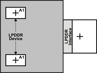 Figure 7-35 LPDDR Keepout Region
7.7.2.1.2.6 Bulk Bypass Capacitors
Bulk bypass capacitors are required for moderate speed bypassing of the LPDDR and other circuitry. Table 7-36 contains the minimum numbers and capacitance required for the bulk bypass capacitors. Note that this table only covers the bypass needs of the AM335x LPDDR interface and LPDDR devices. Additional bulk bypass capacitance may be needed for other circuitry.
Table 7-36 Bulk Bypass Capacitors(1)
| NO. | PARAMETER | MIN | MAX | UNIT |
|---|---|---|---|---|
| 1 | AM335x VDDS_DDR bulk bypass capacitor count | 1 | Devices | |
| 2 | AM335x VDDS_DDR bulk bypass total capacitance | 10 | μF | |
| 3 | LPDDR#1 bulk bypass capacitor count | 1 | Devices | |
| 4 | LPDDR#1 bulk bypass total capacitance | 10 | μF | |
| 5 | LPDDR#2 bulk bypass capacitor count(2) | 1 | Devices | |
| 6 | LPDDR#2 bulk bypass total capacitance(2) | 10 | μF |
- These devices should be placed near the device they are bypassing, but preference should be given to the placement of the high-speed (HS) bypass capacitors.
- Only used when two LPDDR devices are used.
7.7.2.1.2.7 High-Speed Bypass Capacitors
High-speed (HS) bypass capacitors are critical for proper LPDDR interface operation. It is particularly important to minimize the parasitic series inductance of the HS bypass capacitors, the AM335x device LPDDR power, and the AM335x device LPDDR ground connections. Table 7-37 contains the specification for the HS bypass capacitors as well as for the power connections on the PCB.
Table 7-37 High-Speed Bypass Capacitors
| NO. | PARAMETER | MIN | MAX | UNIT |
|---|---|---|---|---|
| 1 | HS bypass capacitor package size(1) | 0402 | 10 mils | |
| 2 | Distance from HS bypass capacitor to device being bypassed | 250 | mils | |
| 3 | Number of connection vias for each HS bypass capacitor(2) | 2 | Vias | |
| 4 | Trace length from bypass capacitor contact to connection via | 30 | mils | |
| 5 | Number of connection vias for each AM335x VDDS_DDR and VSS terminal | 1 | Vias | |
| 6 | Trace length from AM335x VDDS_DDR and VSS terminal to connection via | 35 | mils | |
| 7 | Number of connection vias for each LPDDR device power and ground terminal | 1 | Vias | |
| 8 | Trace length from LPDDR device power and ground terminal to connection via | 35 | mils | |
| 9 | AM335x VDDS_DDR HS bypass capacitor count(3) | 10 | Devices | |
| 10 | AM335x VDDS_DDR HS bypass capacitor total capacitance | 0.6 | μF | |
| 11 | LPDDR device HS bypass capacitor count(3)(4) | 8 | Devices | |
| 12 | LPDDR device HS bypass capacitor total capacitance(4) | 0.4 | μF |
- LxW, 10-mil units; for example, a 0402 is a 40x20-mil surface-mount capacitor.
- An additional HS bypass capacitor can share the connection vias only if it is mounted on the opposite side of the board.
- These devices should be placed as close as possible to the device being bypassed.
- Per LPDDR device.
7.7.2.1.2.8 Net Classes
Table 7-38 lists the clock net classes for the LPDDR interface. Table 7-39 lists the signal net classes, and associated clock net classes, for the signals in the LPDDR interface. These net classes are used for the termination and routing rules that follow.
Table 7-38 Clock Net Class Definitions
| CLOCK NET CLASS | AM335x PIN NAMES |
|---|---|
| CK | DDR_CK and DDR_CKn |
| DQS0 | DDR_DQS0 |
| DQS1 | DDR_DQS1 |
Table 7-39 Signal Net Class Definitions
| SIGNAL NET CLASS | ASSOCIATED CLOCK NET CLASS |
AM335x PIN NAMES |
|---|---|---|
| ADDR_CTRL | CK | DDR_BA[1:0], DDR_A[15:0], DDR_CSn0, DDR_CASn, DDR_RASn, DDR_WEn, DDR_CKE |
| DQ0 | DQS0 | DDR_D[7:0], DDR_DQM0 |
| DQ1 | DQS1 | DDR_D[15:8], DDR_DQM1 |
7.7.2.1.2.9 LPDDR Signal Termination
There is no specific need for adding terminations on the LPDDR interface. However, system designers may evaluate the need for serial terminators for EMI and overshoot reduction. Placement of serial terminations for DQS[x] and DQ[x] net class signals should be determined based on PCB analysis. Placement of serial terminations for ADDR_CTRL net class signals should be close to the AM335x device. Table 7-40 shows the specifications for the serial terminators in such cases.
Table 7-40 LPDDR Signal Terminations
| NO. | PARAMETER | MIN | TYP | MAX | UNIT |
|---|---|---|---|---|---|
| 1 | CK net class(1) | 0 | 22 | Zo(2) | Ω |
| 2 | ADDR_CTRL net class(1)(3)(4) | 0 | 22 | Zo(2) | Ω |
| 3 | DQS0, DQS1, DQ0, and DQ1 net classes | 0 | 22 | Zo(2) | Ω |
- Only series termination is permitted.
- Zo is the LPDDR PCB trace characteristic impedance.
- Series termination values larger than typical only recommended to address EMI issues.
- Series termination values should be uniform across net class.
7.7.2.1.3 LPDDR CK and ADDR_CTRL Routing
Figure 7-36 shows the topology of the routing for the CK and ADDR_CTRL net classes. The length of signal path AB and AC should be minimized with emphasis to minimize lengths C and D such that length A is the majority of the total length of signal path AB and AC.
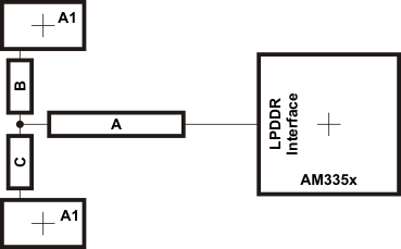 Figure 7-36 CK and ADDR_CTRL Routing and Topology
Table 7-41 CK and ADDR_CTRL Routing Specification(1)(2)
| NO. | PARAMETER | MIN | TYP | MAX | UNIT |
|---|---|---|---|---|---|
| 1 | Center-to-center CK spacing | 2w | |||
| 2 | CK differential pair skew length mismatch(2)(3) | 25 | mils | ||
| 3 | CK B-to-CK C skew length mismatch | 25 | mils | ||
| 4 | Center-to-center CK to other LPDDR trace spacing(4) | 4w | |||
| 5 | CK and ADDR_CTRL nominal trace length(5) | CACLM-50 | CACLM | CACLM+50 | mils |
| 6 | ADDR_CTRL-to-CK skew length mismatch | 100 | mils | ||
| 7 | ADDR_CTRL-to-ADDR_CTRL skew length mismatch | 100 | mils | ||
| 8 | Center-to-center ADDR_CTRL to other LPDDR trace spacing(4) | 4w | |||
| 9 | Center-to-center ADDR_CTRL to other ADDR_CTRL trace spacing(4) | 3w | |||
| 10 | ADDR_CTRL A-to-B and ADDR_CTRL A-to-C skew length mismatch(2) | 100 | mils | ||
| 11 | ADDR_CTRL B-to-C skew length mismatch | 100 | mils |
- CK represents the clock net class, and ADDR_CTRL represents the address and control signal net class.
- Series terminator, if used, should be located closest to the AM335x device.
- Differential impedance should be Zo x 2, where Zo is the single-ended impedance defined in Table 7-34.
- Center-to-center spacing is allowed to fall to minimum (w) for up to 500 mils of routed length to accommodate BGA escape and routing congestion.
- CACLM is the longest Manhattan distance of the CK and ADDR_CTRL net classes.
Figure 7-37 shows the topology and routing for the DQS[x] and DQ[x] net classes; the routes are point to point. Skew matching across bytes is not needed nor recommended.
![AM3359 AM3358 AM3357 AM3356 AM3354 AM3352 AM3351 DQS[x] and DQ[x]
Routing and Topology AM3359 AM3358 AM3357 AM3356 AM3354 AM3352 AM3351 lpddr_dqs_dx_rout_topo_sprs717.gif](/ods/images/JAJSDZ0J/lpddr_dqs_dx_rout_topo_sprs717.gif) Figure 7-37 DQS[x] and DQ[x] Routing and Topology
Figure 7-37 DQS[x] and DQ[x] Routing and Topology
Table 7-42 DQS[x] and DQ[x] Routing Specification(1)
| NO. | PARAMETER | MIN | TYP | MAX | UNIT |
|---|---|---|---|---|---|
| 1 | Center-to-center DQS[x] spacing | 2w | |||
| 2 | Center-to-center DDR_DQS[x] to other LPDDR trace spacing(2) | 4w | |||
| 3 | DQS[x] and DQ[x] nominal trace length(3) | DQLM-50 | DQLM | DQLM+50 | mils |
| 4 | DQ[x]-to-DQS[x] skew length mismatch(3) | 100 | mils | ||
| 5 | DQ[x]-to-DQ[x] skew length mismatch(3) | 100 | mils | ||
| 6 | Center-to-center DQ[x] to other LPDDR trace spacing(2)(4) | 4w | |||
| 7 | Center-to-center DQ[x] to other DQ[x] trace spacing(2)(5) | 3w |
- DQS[x] represents the DQS0 and DQS1 clock net classes, and DQ[x] represents the DQ0 and DQ1 signal net classes.
- Center-to-center spacing is allowed to fall to minimum (w) for up to 500 mils of routed length to accommodate BGA escape and routing congestion.
- There is no requirement for skew matching between data bytes; that is, from net classes DQS0 and DQ0 to net classes DQS1 and DQ1.
- Signals from one DQ net class should be considered other LPDDR traces to another DQ net class.
- DQLM is the longest Manhattan distance of each of the DQS[x] and DQ[x] net classes.
7.7.2.2 DDR2 Routing Guidelines
7.7.2.2.1 Board Designs
TI only supports board designs that follow the guidelines outlined in this document. Table 7-43 and Figure 7-38 show the switching characteristics and timing diagram for the DDR2 memory interface.
Table 7-43 Switching Characteristics for DDR2 Memory Interface
| NO. | PARAMETER | MIN | MAX | UNIT | |
|---|---|---|---|---|---|
| 1 | tc(DDR_CK)
tc(DDR_CKn) |
Cycle time, DDR_CK and DDR_CKn | 3.75 | 8(1) | ns |
7.7.2.2.2 DDR2 Interface
This section provides the timing specification for the DDR2 interface as a PCB design and manufacturing specification. The design rules constrain PCB trace length, PCB trace skew, signal integrity, cross-talk, and signal timing. These rules, when followed, result in a reliable DDR2 memory system without the need for a complex timing closure process. For more information regarding the guidelines for using this DDR2 specification, see Understanding TI’s PCB Routing Rule-Based DDR Timing Specification. This application report provides generic guidelines and approach. All the specifications provided in the data manual take precedence over the generic guidelines and must be adhered to for a reliable DDR2 interface operation.
7.7.2.2.2.1 DDR2 Interface Schematic
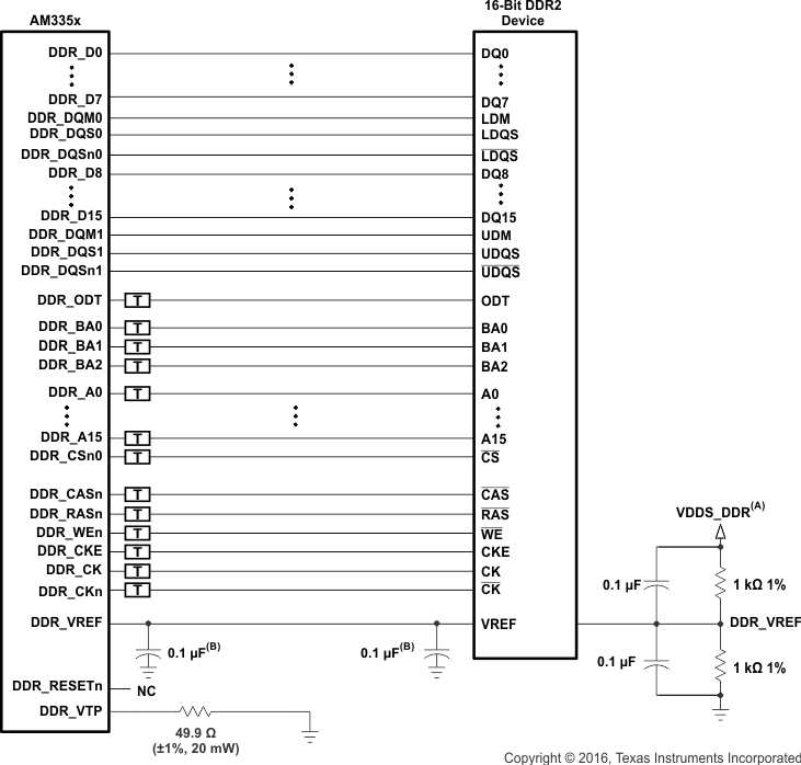
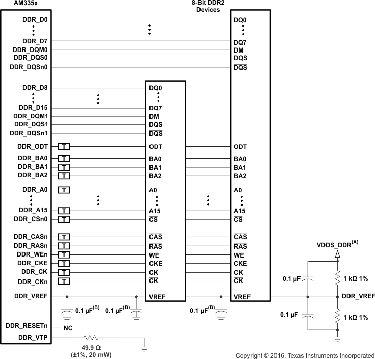
Figure 7-39 shows the schematic connections for 16-bit interface on the AM335x device using one x16 DDR2 device and Figure 7-40 shows the schematic connections for 16-bit interface on the AM335x device using two x8 DDR2 devices. The AM335x DDR2 memory interface only supports 16-bit-wide mode of operation. The AM335x device can only source one load connected to the DQS[x] and DQ[x] net class signals and two loads connected to the CK and ADDR_CTRL net class signals. For more information related to net classes, see Section 7.7.2.2.2.8.
7.7.2.2.2.2 Compatible JEDEC DDR2 Devices
Table 7-44 shows the parameters of the JEDEC DDR2 devices that are compatible with this interface. Generally, the DDR2 interface is compatible with x16 or x8 DDR2-533 speed grade DDR2 devices.
Table 7-44 Compatible JEDEC DDR2 Devices (Per Interface)(1)
| NO. | PARAMETER | MIN | MAX | UNIT |
|---|---|---|---|---|
| 1 | JEDEC DDR2 device speed grade(2) | DDR2-533 | ||
| 2 | JEDEC DDR2 device bit width | x8 | x16 | bits |
| 3 | JEDEC DDR2 device count | 1 | 2 | devices |
| 4 | JEDEC DDR2 device terminal count(3) | 60 | 84 | terminals |
- If the DDR2 interface is operated with a clock frequency less than 266 MHz, lower-speed grade DDR2 devices may be used if the minimum clock period specified for the DDR2 device is less than or equal to the minimum clock period selected for the AM335x DDR2 interface.
- Higher DDR2 speed grades are supported due to inherent JEDEC DDR2 backward compatibility.
- 92-terminal devices are also supported for legacy reasons. New designs will migrate to 84-terminal DDR2 devices. Electrically, the 92- and 84-terminal DDR2 devices are the same.
7.7.2.2.2.3 PCB Stackup
The minimum stackup required for routing the AM335x device is a 4-layer stackup as shown in Table 7-45. Additional layers may be added to the PCB stackup to accommodate other circuitry, enhance signal integrity and electromagnetic interference performance, or to reduce the size of the PCB footprint.
Table 7-45 Minimum PCB Stackup(1)
| LAYER | TYPE | DESCRIPTION |
|---|---|---|
| 1 | Signal | Top signal routing |
| 2 | Plane | Ground |
| 3 | Plane | Split power plane |
| 4 | Signal | Bottom signal routing |
- All signals that have critical signal integrity requirements should be routed first on layer 1. It may not be possible to route all of these signals on layer 1, therefore requiring routing of some signals on layer 4. When this is done, the signal routes on layer 4 must not cross splits in the power plane.
Complete stackup specifications are provided in Table 7-46.
Table 7-46 PCB Stackup Specifications(1)
| NO. | PARAMETER | MIN | TYP | MAX | UNIT | |
|---|---|---|---|---|---|---|
| 1 | PCB routing and plane layers | 4 | ||||
| 2 | Signal routing layers | 2 | ||||
| 3 | Full ground layers under DDR2 routing region | 1 | ||||
| 4 | Number of ground plane cuts allowed within DDR2 routing region | 0 | ||||
| 5 | Full VDDS_DDR power reference layers under DDR2 routing region | 1 | ||||
| 6 | Number of layers between DDR2 routing layer and reference ground plane | 0 | ||||
| 7 | PCB routing feature size | 4 | mils | |||
| 8 | PCB trace width, w | 4 | mils | |||
| 9 | PCB BGA escape via pad size(2) | 18 | 20 | mils | ||
| 10 | PCB BGA escape via hole size(2) | 10 | mils | |||
| 11 | Single-ended impedance, Zo(3) | 50 | 75 | Ω | ||
| 12 | Impedance control(4)(5) | Zo-5 | Zo | Zo+5 | Ω | |
- For the DDR2 device BGA pad size, see the DDR2 device manufacturer documentation.
- A 20-10 via may be used if enough power routing resources are available. An 18-10 via allows for more flexible power routing to the AM335x device.
- Zo is the nominal singled-ended impedance selected for the PCB.
- This parameter specifies the AC characteristic impedance tolerance for each segment of a PCB signal trace relative to the chosen Zo defined by the single-ended impedance parameter.
- Tighter impedance control is required to ensure flight time skew is minimal.
7.7.2.2.2.4 Placement
Figure 7-41 shows the required placement for the DDR2 devices. The dimensions for this figure are defined in Table 7-47. The placement does not restrict the side of the PCB on which the devices are mounted. The ultimate purpose of the placement is to limit the maximum trace lengths and allow for proper routing space. For single-memory DDR2 systems, the second DDR2 device is omitted from the placement.
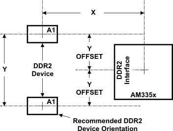 Figure 7-41 AM335x Device and DDR2 Device Placement
Table 7-47 Placement Specifications(1)
| NO. | PARAMETER | MIN | MAX | UNIT |
|---|---|---|---|---|
| 1 | X(2)(3) | 1750 | mils | |
| 2 | Y(2)(3) | 1280 | mils | |
| 3 | Y Offset(2)(3)(4) | 650 | mils | |
| 4 | Clearance from non-DDR2 signal to DDR2 keepout region(5)(6) | 4 | w |
- DDR2 keepout region to encompass entire DDR2 routing area.
- For dimension definitions, see Figure 7-41.
- Measurements from center of the AM335x device to center of the DDR2 device.
- For single-memory systems, it is recommended that Y offset be as small as possible.
- w is defined as the signal trace width.
- Non-DDR2 signals allowed within DDR2 keepout region provided they are separated from DDR2 routing layers by a ground plane.
7.7.2.2.2.5 DDR2 Keepout Region
The region of the PCB used for the DDR2 circuitry must be isolated from other signals. The DDR2 keepout region is defined for this purpose and is shown in Figure 7-42. This region should encompass all DDR2 circuitry and the region size varies with component placement and DDR2 routing. Additional clearances required for the keepout region are shown in Table 7-47. Non-DDR2 signals must not be routed on the same signal layer as DDR2 signals within the DDR2 keepout region. Non-DDR2 signals may be routed in the region provided they are routed on layers separated from DDR2 signal layers by a ground layer. No breaks should be allowed in the reference ground or VDDS_DDR power plane in this region. In addition, the VDDS_DDR power plane should cover the entire keepout region.
7.7.2.2.2.6 Bulk Bypass Capacitors
Bulk bypass capacitors are required for moderate speed bypassing of the DDR2 and other circuitry. Table 7-48 contains the minimum numbers and capacitance required for the bulk bypass capacitors. Note that this table only covers the bypass needs of the AM335x DDR2 interface and DDR2 devices. Additional bulk bypass capacitance may be needed for other circuitry.
Table 7-48 Bulk Bypass Capacitors(1)
| NO. | PARAMETER | MIN | MAX | UNIT |
|---|---|---|---|---|
| 1 | AM335x VDDS_DDR bulk bypass capacitor count | 1 | devices | |
| 2 | AM335x VDDS_DDR bulk bypass total capacitance | 10 | μF | |
| 3 | DDR2 number 1 bulk bypass capacitor count | 1 | devices | |
| 4 | DDR2 number 1 bulk bypass total capacitance | 10 | μF | |
| 5 | DDR2 number 2 bulk bypass capacitor count(2) | 1 | devices | |
| 6 | DDR2 number 2 bulk bypass total capacitance(2) | 10 | μF |
7.7.2.2.2.7 High-Speed (HS) Bypass Capacitors
HS bypass capacitors are critical for proper DDR2 interface operation. It is particularly important to minimize the parasitic series inductance of the HS bypass capacitors, the AM335x device DDR2 power, and the AM335x device DDR2 ground connections. Table 7-49 contains the specification for the HS bypass capacitors as well as for the power connections on the PCB.
Table 7-49 HS Bypass Capacitors
| NO. | PARAMETER | MIN | MAX | UNIT |
|---|---|---|---|---|
| 1 | HS bypass capacitor package size(1) | 0402 | 10 mils | |
| 2 | Distance from HS bypass capacitor to device being bypassed | 250 | mils | |
| 3 | Number of connection vias for each HS bypass capacitor(2) | 2 | vias | |
| 4 | Trace length from bypass capacitor contact to connection via | 30 | mils | |
| 5 | Number of connection vias for each AM335x VDDS_DDR and VSS terminal | 1 | vias | |
| 6 | Trace length from AM335x VDDS_DDR and VSS terminal to connection via | 35 | mils | |
| 7 | Number of connection vias for each DDR2 device power and ground terminal | 1 | vias | |
| 8 | Trace length from DDR2 device power and ground terminal to connection via | 35 | mils | |
| 9 | AM335x VDDS_DDR HS bypass capacitor count(3) | 10 | devices | |
| 10 | AM335x VDDS_DDR HS bypass capacitor total capacitance | 0.6 | μF | |
| 11 | DDR2 device HS bypass capacitor count(3)(4) | 8 | devices | |
| 12 | DDR2 device HS bypass capacitor total capacitance(4) | 0.4 | μF |
- LxW, 10-mil units; for example, a 0402 is a 40x20-mil surface-mount capacitor.
- An additional HS bypass capacitor can share the connection vias only if it is mounted on the opposite side of the board.
- These devices should be placed as close as possible to the device being bypassed.
- Per DDR2 device.
7.7.2.2.2.8 Net Classes
Table 7-50 lists the clock net classes for the DDR2 interface. Table 7-51 lists the signal net classes, and associated clock net classes, for the signals in the DDR2 interface. These net classes are used for the termination and routing rules that follow.
7.7.2.2.2.9 DDR2 Signal Termination
Signal terminations are required on the CK and ADDR_CTRL net class signals. Serial terminations should be used on the CK and ADDR_CTRL lines and is the preferred termination scheme. On-device terminations (ODTs) are required on the DQS[x] and DQ[x] net class signals. They should be enabled to ensure signal integrity. Table 7-52 shows the specifications for the series terminators. Placement of serial terminations for ADDR_CTRL net class signals should be close to the AM335x device.
Table 7-52 DDR2 Signal Terminations
| NO. | PARAMETER | MIN | TYP | MAX | UNIT |
|---|---|---|---|---|---|
| 1 | CK net class(1) | 0 | 10 | Ω | |
| 2 | ADDR_CTRL net class(1)(2)(3) | 0 | 22 | Zo(4) | Ω |
| 3 | DQS0, DQS1, DQ0, and DQ1 net classes(5) | N/A | N/A | Ω |
- Only series termination is permitted.
- Series termination values larger than typical only recommended to address EMI issues.
- Series termination values should be uniform across net class.
- Zo is the DDR2 PCB trace characteristic impedance.
- No external termination resistors are allowed and ODT must be used for these net classes.
If the DDR2 interface is operated at a lower frequency (<200-MHz clock rate), on-device terminations are not specifically required for the DQS[x] and DQ[x] net class signals and serial terminations for the CK and ADDR_CTRL net class signals are not mandatory. System designers may evaluate the need for serial terminators for EMI and overshoot reduction. Placement of serial terminations for DQS[x] and DQ[x] net class signals should be determined based on PCB analysis. Placement of serial terminations for ADDR_CTRL net class signals should be close to the AM335x device. Table 7-53 shows the specifications for the serial terminators in such cases.
Table 7-53 Lower-Frequency DDR2 Signal Terminations
| NO. | PARAMETER | MIN | TYP | MAX | UNIT |
|---|---|---|---|---|---|
| 1 | CK net class(1) | 0 | 22 | Zo(2) | Ω |
| 2 | ADDR_CTRL net class(1)(3)(4) | 0 | 22 | Zo(2) | Ω |
| 3 | DQS0, DQS1, DQ0, and DQ1 net classes | 0 | 22 | Zo(2) | Ω |
- Only series termination is permitted.
- Zo is the DDR2 PCB trace characteristic impedance.
- Series termination values larger than typical only recommended to address EMI issues.
- Series termination values should be uniform across net class.
7.7.2.2.2.10 DDR_VREF Routing
DDR_VREF is used as a reference by the input buffers of the DDR2 memories as well as the AM335x device. DDR_VREF is intended to be half the DDR2 power supply voltage and should be created using a resistive divider as shown in Figure 7-39 and Figure 7-40. TI does not recommend other methods of creating DDR_VREF. Figure 7-43 shows the layout guidelines for DDR_VREF.
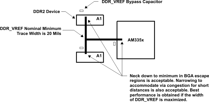 Figure 7-43 DDR_VREF Routing and Topology
7.7.2.2.3 DDR2 CK and ADDR_CTRL Routing
Figure 7-44 shows the topology of the routing for the CK and ADDR_CTRL net classes. The length of signal path AB and AC should be minimized with emphasis to minimize lengths C and D such that length A is the majority of the total length of signal path AB and AC.
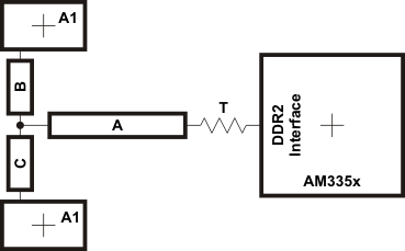 Figure 7-44 CK and ADDR_CTRL Routing and Topology
Table 7-54 CK and ADDR_CTRL Routing Specification(1)(2)
| NO. | PARAMETER | MIN | TYP | MAX | UNIT |
|---|---|---|---|---|---|
| 1 | Center-to-center CK spacing | 2w | |||
| 2 | CK differential pair skew length mismatch(2)(3) | 25 | mils | ||
| 3 | CK B-to-CK C skew length mismatch | 25 | mils | ||
| 4 | Center-to-center CK to other DDR2 trace spacing(4) | 4w | |||
| 5 | CK and ADDR_CTRL nominal trace length(5) | CACLM-50 | CACLM | CACLM+50 | mils |
| 6 | ADDR_CTRL-to-CK skew length mismatch | 100 | mils | ||
| 7 | ADDR_CTRL-to-ADDR_CTRL skew length mismatch | 100 | mils | ||
| 8 | Center-to-center ADDR_CTRL to other DDR2 trace spacing(4) | 4w | |||
| 9 | Center-to-center ADDR_CTRL to other ADDR_CTRL trace spacing(4) | 3w | |||
| 10 | ADDR_CTRL A-to-B and ADDR_CTRL A-to-C skew length mismatch(2) | 100 | mils | ||
| 11 | ADDR_CTRL B-to-C skew length mismatch | 100 | mils |
- CK represents the clock net class, and ADDR_CTRL represents the address and control signal net class.
- Series terminator, if used, should be located closest to the AM335x device.
- Differential impedance should be Zo x 2, where Zo is the single-ended impedance defined in Table 7-46.
- Center-to-center spacing is allowed to fall to minimum (w) for up to 500 mils of routed length to accommodate BGA escape and routing congestion.
- CACLM is the longest Manhattan distance of the CK and ADDR_CTRL net classes.
Figure 7-45 shows the topology and routing for the DQS[x] and DQ[x] net classes; the routes are point to point. Skew matching across bytes is not needed nor recommended.
Table 7-55 DQS[x] and DQ[x] Routing Specification(1)
| NO. | PARAMETER | MIN | TYP | MAX | UNIT |
|---|---|---|---|---|---|
| 1 | Center-to-center DQS[x] spacing | 2w | |||
| 2 | DQS[x] differential pair skew length mismatch(2) | 25 | mils | ||
| 3 | Center-to-center DDR_DQS[x] to other DDR2 trace spacing(3) | 4w | |||
| 4 | DQS[x] and DQ[x] nominal trace length(4) | DQLM-50 | DQLM | DQLM+50 | mils |
| 5 | DQ[x]-to-DQS[x] skew length mismatch(4) | 100 | mils | ||
| 6 | DQ[x]-to-DQ[x] skew length mismatch(4) | 100 | mils | ||
| 7 | Center-to-center DQ[x] to other DDR2 trace spacing(3)(5) | 4w | |||
| 8 | Center-to-center DQ[x] to other DQ[x] trace spacing(3)(6) | 3w |
- DQS[x] represents the DQS0 and DQS1 clock net classes, and DQ[x] represents the DQ0 and DQ1 signal net classes.
- Differential impedance should be Zo x 2, where Zo is the single-ended impedance defined in Table 7-46.
- Center-to-center spacing is allowed to fall to minimum (w) for up to 500 mils of routed length to accommodate BGA escape and routing congestion.
- There is no requirement for skew matching between data bytes; that is, from net classes DQS0 and DQ0 to net classes DQS1 and DQ1.
- Signals from one DQ net class should be considered other DDR2 traces to another DQ net class.
- DQLM is the longest Manhattan distance of each of the DQS[x] and DQ[x] net classes.
7.7.2.3 DDR3 and DDR3L Routing Guidelines
NOTE
All references to DDR3 in this section apply to DDR3 and DDR3L devices, unless otherwise noted.
7.7.2.3.1 Board Designs
TI only supports board designs using DDR3 memory that follow the guidelines in this document. The switching characteristics and timing diagram for the DDR3 memory interface are shown in Table 7-56 and Figure 7-46.
Table 7-56 Switching Characteristics for DDR3 Memory Interface
| NO. | PARAMETER | MIN | MAX | UNIT | |
|---|---|---|---|---|---|
| 1 | tc(DDR_CK)
tc(DDR_CKn) |
Cycle time, DDR_CK and DDR_CKn | 2.5 | 3.3(1) | ns |
- The JEDEC JESD79-3F Standard defines the maximum clock period of 3.3 ns for all standard-speed bin DDR3 and DDR3L memory devices. Therefore, all standard-speed bin DDR3 and DDR3L memory devices are required to operate at 303 MHz.
 Figure 7-46 DDR3 Memory Interface Clock Timing
7.7.2.3.1.1 DDR3 versus DDR2
This specification only covers AM335x PCB designs that use DDR3 memory. Designs using DDR2 memory should use the DDR2 routing guidleines described in Section 7.7.2.2. While similar, the two memory systems have different requirements. It is currently not possible to design one PCB that meets the requirements of both DDR2 and DDR3.
7.7.2.3.2 DDR3 Device Combinations
Because there are several possible combinations of device counts and single-side or dual-side mounting, Table 7-57 summarizes the supported device configurations.
Table 7-57 Supported DDR3 Device Combinations
| NUMBER OF DDR3 DEVICES | DDR3 DEVICE WIDTH (BITS) | MIRRORED? | DDR3 EMIF WIDTH (BITS) |
|---|---|---|---|
| 1 | 16 | N | 16 |
| 2 | 8 | Y(1) | 16 |
7.7.2.3.3 DDR3 Interface
This section provides the timing specification for the DDR3 interface as a PCB design and manufacturing specification. The design rules constrain PCB trace length, PCB trace skew, signal integrity, cross-talk, and signal timing. These rules, when followed, result in a reliable DDR3 memory system without the need for a complex timing closure process. For more information regarding the guidelines for using this DDR3 specification, see Understanding TI's PCB Routing Rule-Based DDR Timing Specification. This application report provides generic guidelines and approach. All the specifications provided in the data manual take precedence over the generic guidelines and must be adhered to for a reliable DDR3 interface operation.
7.7.2.3.3.1 DDR3 Interface Schematic
The DDR3 interface schematic varies, depending upon the width of the DDR3 devices used. Figure 7-47 shows the schematic connections for 16-bit interface on the AM335x device using one x16 DDR3 device and Figure 7-49 shows the schematic connections for 16-bit interface on the AM335x device using two x8 DDR3 devices. The AM335x DDR3 memory interface only supports 16-bit wide mode of operation. The AM335x device can only source one load connected to the DQS[x] and DQ[x] net class signals and two loads connected to the CK and ADDR_CTRL net class signals. For more information related to net classes, see Section 7.7.2.3.3.8.
7.7.2.3.3.2 Compatible JEDEC DDR3 Devices
Table 7-58 shows the parameters of the JEDEC DDR3 devices that are compatible with this interface.
Table 7-58 Compatible JEDEC DDR3 Devices (Per Interface)
| NO. | PARAMETER | TEST CONDITIONS | MIN | MAX | UNIT |
|---|---|---|---|---|---|
| 1 | JEDEC DDR3 device speed grade | tC(DDR_CK) and tC(DDR_CKn) = 3.3 ns | DDR3-800 | ||
| tC(DDR_CK) and tC(DDR_CKn) = 2.5 ns | DDR3-1600 | ||||
| 2 | JEDEC DDR3 device bit width | x8 | x16 | bits | |
| 3 | JEDEC DDR3 device count(1) | 1 | 2 | devices |
- For valid DDR3 device configurations and device counts, see Section 7.7.2.3.3.1, Figure 7-47, and Figure 7-49.
7.7.2.3.3.3 PCB Stackup
The minimum stackup for routing the DDR3 interface is a four-layer stack up as shown in Table 7-59. Additional layers may be added to the PCB stackup to accommodate other circuitry, enhance signal integrity and electromagnetic interference performance, or to reduce the size of the PCB footprint.
Table 7-59 Minimum PCB Stackup(1)
| LAYER | TYPE | DESCRIPTION |
|---|---|---|
| 1 | Signal | Top signal routing |
| 2 | Plane | Ground |
| 3 | Plane | Split Power Plane |
| 4 | Signal | Bottom signal routing |
- All signals that have critical signal integrity requirements should be routed first on layer 1. It may not be possible to route all of these signals on layer 1, therefore requiring routing of some signals on layer 4. When this is done, the signal routes on layer 4 must not cross splits in the power plane.
Table 7-60 PCB Stackup Specifications(1)
| NO. | PARAMETER | MIN | TYP | MAX | UNIT | |
|---|---|---|---|---|---|---|
| 1 | PCB routing and plane layers | 4 | ||||
| 2 | Signal routing layers | 2 | ||||
| 3 | Full ground reference layers under DDR3 routing region(2) | 1 | ||||
| 4 | Full VDDS_DDR power reference layers under the DDR3 routing region(2) | 1 | ||||
| 5 | Number of reference plane cuts allowed within DDR3 routing region(3) | 0 | ||||
| 6 | Number of layers between DDR3 routing layer and reference plane(4) | 0 | ||||
| 7 | PCB routing feature size | 4 | mils | |||
| 8 | PCB trace width, w | 4 | mils | |||
| 9 | PCB BGA escape via pad size(5) | 18 | 20 | mils | ||
| 10 | PCB BGA escape via hole size | 10 | mils | |||
| 11 | Single-ended impedance, Zo(6) | 50 | 75 | Ω | ||
| 12 | Impedance control(7)(8) | Zo-5 | Zo | Zo+5 | Ω | |
- For the DDR3 device BGA pad size, see the DDR3 device manufacturer documentation.
- Ground reference layers are preferred over power reference layers. Be sure to include bypass capacitors to accommodate reference layer return current as the trace routes switch routing layers.
- No traces should cross reference plane cuts within the DDR3 routing region. High-speed signal traces crossing reference plane cuts create large return current paths which can lead to excessive crosstalk and EMI radiation.
- Reference planes are to be directly adjacent to the signal plane to minimize the size of the return current loop.
- An 18-mil pad assumes Via Channel is the most economical BGA escape. A 20-mil pad may be used if additional layers are available for power routing. An 18-mil pad is required for minimum layer count escape.
- Zo is the nominal singled-ended impedance selected for the PCB.
- This parameter specifies the AC characteristic impedance tolerance for each segment of a PCB signal trace relative to the chosen Zo defined by the single-ended impedance parameter.
- Tighter impedance control is required to ensure flight time skew is minimal.
7.7.2.3.3.4 Placement
Figure 7-50 shows the required placement for the AM335x device as well as the DDR3 devices. The dimensions for this figure are defined in Table 7-61. The placement does not restrict the side of the PCB on which the devices are mounted. The ultimate purpose of the placement is to limit the maximum trace lengths and allow for proper routing space.
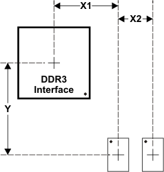 Figure 7-50 Placement Specifications
Table 7-61 Placement Specifications(1)
| NO. | PARAMETER | MIN | MAX | UNIT |
|---|---|---|---|---|
| 1 | X1(2)(3)(4) | 1000 | mils | |
| 2 | X2(2)(3) | 600 | mils | |
| 3 | Y Offset(2)(3)(4) | 1500 | mils | |
| 4 | Clearance from non-DDR3 signal to DDR3 keepout region(5)(6) | 4 | w |
- DDR3 keepout region to encompass entire DDR3 routing area.
- For dimension definitions, see Figure 7-50.
- Measurements from center of the AM335x device to center of the DDR3 device.
- Minimizing X1 and Y improves timing margins.
- w is defined as the signal trace width.
- Non-DDR3 signals allowed within DDR3 keepout region provided they are separated from DDR3 routing layers by a ground plane.
7.7.2.3.3.5 DDR3 Keepout Region
The region of the PCB used for DDR3 circuitry must be isolated from other signals. The DDR3 keepout region is defined for this purpose and is shown in Figure 7-51. This region should encompass all DDR3 circuitry and the region size varies with component placement and DDR3 routing. Additional clearances required for the keepout region are shown in Table 7-61. Non-DDR3 signals must not be routed on the same signal layer as DDR3 signals within the DDR3 keepout region. Non-DDR3 signals may be routed in the region provided they are routed on layers separated from DDR3 signal layers by a ground layer. No breaks should be allowed in the reference ground or VDDS_DDR power plane in this region. In addition, the VDDS_DDR power plane should cover the entire keepout region.
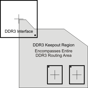 Figure 7-51 DDR3 Keepout Region
7.7.2.3.3.6 Bulk Bypass Capacitors
Bulk bypass capacitors are required for moderate speed bypassing of the DDR3 and other circuitry. Table 7-62 contains the minimum numbers and capacitance required for the bulk bypass capacitors. Note that this table only covers the bypass needs of the AM335x DDR3 interface and DDR3 devices. Additional bulk bypass capacitance may be needed for other circuitry.
Table 7-62 Bulk Bypass Capacitors(1)
| NO. | PARAMETER | MIN | MAX | UNIT |
|---|---|---|---|---|
| 1 | AM335x VDDS_DDR bulk bypass capacitor count | 2 | devices | |
| 2 | AM335x VDDS_DDR bulk bypass total capacitance | 20 | μF | |
| 3 | DDR3 number 1 bulk bypass capacitor count | 2 | devices | |
| 4 | DDR3 number 1 bulk bypass total capacitance | 20 | μF | |
| 5 | DDR3 number 2 bulk bypass capacitor count(2) | 2 | devices | |
| 6 | DDR3 number 2 bulk bypass total capacitance(2) | 20 | μF |
- These devices should be placed near the devices they are bypassing, but preference should be given to the placement of the high-speed (HS) bypass capacitors and DDR3 signal routing.
- Only used when two DDR3 devices are used.
7.7.2.3.3.7 High-Speed Bypass Capacitors
High-speed (HS) bypass capacitors are critical for proper DDR3 interface operation. It is particularly important to minimize the parasitic series inductance of the HS bypass capacitors, the AM335x device DDR3 power, and the AM335x device DDR3 ground connections. Table 7-63 contains the specification for the HS bypass capacitors as well as for the power connections on the PCB. Generally speaking, it is good to:
- Fit as many HS bypass capacitors as possible.
- Minimize the distance from the bypass capacitor to the power terminals being bypassed.
- Use the smallest physical sized capacitors possible with the highest capacitance readily available.
- Connect the bypass capacitor pads to their vias using the widest traces possible and using the largest hole size via possible.
- Minimize via sharing. Note the limits on via sharing shown in Table 7-63.
Table 7-63 High-Speed Bypass Capacitors
| NO. | PARAMETER | MIN | TYP | MAX | UNIT |
|---|---|---|---|---|---|
| 1 | HS bypass capacitor package size(1) | 0201 | 0402 | 10 mils | |
| 2 | Distance, HS bypass capacitor to AM335x VDDS_DDR and VSS terminal being bypassed(2)(3)(4) | 400 | mils | ||
| 3 | AM335x VDDS_DDR HS bypass capacitor count | 20 | devices | ||
| 4 | AM335x VDDS_DDR HS bypass capacitor total capacitance | 1 | μF | ||
| 5 | Trace length from AM335x VDDS_DDR and VSS terminal to connection via(2) | 35 | 70 | mils | |
| 6 | Distance, HS bypass capacitor to DDR3 device being bypassed(5) | 150 | mils | ||
| 7 | DDR3 device HS bypass capacitor count(6) | 12 | devices | ||
| 8 | DDR3 device HS bypass capacitor total capacitance(6) | 0.85 | μF | ||
| 9 | Number of connection vias for each HS bypass capacitor(7)(8) | 2 | vias | ||
| 10 | Trace length from bypass capacitor connect to connection via(2)(8) | 35 | 100 | mils | |
| 11 | Number of connection vias for each DDR3 device power and ground terminal(9) | 1 | vias | ||
| 12 | Trace length from DDR3 device power and ground terminal to connection via(2)(7) | 35 | 60 | mils |
- LxW, 10-mil units; for example, a 0402 is a 40x20-mil surface-mount capacitor.
- Closer and shorter is better.
- Measured from the nearest AM335x VDDS_DDR and ground terminal to the center of the capacitor package.
- Three of these capacitors should be located underneath the AM335x device, between the cluster of VDDS_DDR and ground terminals, between the DDR3 interfaces on the package.
- Measured from the DDR3 device power and ground terminal to the center of the capacitor package.
- Per DDR3 device.
- An additional HS bypass capacitor can share the connection vias only if it is mounted on the opposite side of the board. No sharing of vias is permitted on the same side of the board.
- An HS bypass capacitor may share a via with a DDR3 device mounted on the same side of the PCB. A wide trace should be used for the connection and the length from the capacitor pad to the DDR3 device pad should be less than 150 mils.
- Up to two pairs of DDR3 power and ground terminals may share a via.
7.7.2.3.3.7.1 Return Current Bypass Capacitors
Use additional bypass capacitors if the return current reference plane changes due to DDR3 signals hopping from one signal layer to another. The bypass capacitor here provides a path for the return current to hop planes along with the signal. As many of these return current bypass capacitors should be used as possible. Because these are returns for signal current, the signal via size may be used for these capacitors.
7.7.2.3.3.8 Net Classes
Table 7-64 lists the clock net classes for the DDR3 interface. Table 7-65 lists the signal net classes, and associated clock net classes, for signals in the DDR3 interface. These net classes are used for the termination and routing rules that follow.
Table 7-64 Clock Net Class Definitions
| CLOCK NET CLASS | AM335x PIN NAMES |
|---|---|
| CK | DDR_CK and DDR_CKn |
| DQS0 | DDR_DQS0 and DDR_DQSn0 |
| DQS1 | DDR_DQS1 and DDR_DQSn1 |
Table 7-65 Signal Net Class Definitions
| SIGNAL NET CLASS | ASSOCIATED CLOCK NET CLASS | AM335x PIN NAMES |
|---|---|---|
| ADDR_CTRL | CK | DDR_BA[2:0], DDR_A[15:0], DDR_CSn0, DDR_CASn, DDR_RASn, DDR_WEn, DDR_CKE, DDR_ODT |
| DQ0 | DQS0 | DDR_D[7:0], DDR_DQM0 |
| DQ1 | DQS1 | DDR_D[15:8], DDR_DQM1 |
7.7.2.3.3.9 DDR3 Signal Termination
Signal terminations are required for the CK and ADDR_CTRL net class signals. On-device terminations (ODTs) are required on the DQS[x] and DQ[x] net class signals. Detailed termination specifications are covered in the routing rules in the following sections.
Figure 7-48 provides an example DDR3 schematic with a single 16-bit DDR3 memory device that does not have VTT termination on the address and control signals. A typical DDR3 point-to-point topology may provide acceptable signal integrity without VTT termination. System performance should be verified by performing signal integrity analysis using specific PCB design details before implementing this topology.
7.7.2.3.3.10 DDR_VREF Routing
DDR_VREF is used as a reference by the input buffers of the DDR3 memories as well as the AM335x device. DDR_VREF is intended to be half the DDR3 power supply voltage and is typically generated with a voltage divider connected to the VDDS_DDR power supply. It should be routed as a nominal 20-mil wide trace with 0.1 µF bypass capacitors near each device connection. Narrowing of DDR_VREF is allowed to accommodate routing congestion.
7.7.2.3.3.11 VTT
Like DDR_VREF, the nominal value of the VTT supply is half the DDR3 supply voltage. Unlike DDR_VREF, VTT is expected to source and sink current, specifically the termination current for the ADDR_CTRL net class Thevinen terminators. VTT is needed at the end of the address bus and it should be routed as a power sub-plane. VTT should be bypassed near the terminator resistors.
7.7.2.3.4 DDR3 CK and ADDR_CTRL Topologies and Routing Definition
The CK and ADDR_CTRL net classes are routed similarly and are length matched to minimize skew between them. CK is a bit more complicated because it runs at a higher transition rate and is differential. The following subsections show the topology and routing for various DDR3 configurations for CK and ADDR_CTRL. The figures in the following subsections define the terms for the routing specification detailed in Table 7-66.
7.7.2.3.4.1 Two DDR3 Devices
Two DDR3 devices are supported on the DDR3 interface consisting of two x8 DDR3 devices arranged as one 16-bit bank. These two devices may be mounted on a single side of the PCB, or may be mirrored in a pair to save board space at a cost of increased routing complexity and parts on the backside of the PCB.
7.7.2.3.4.1.1 CK and ADDR_CTRL Topologies, Two DDR3 Devices
Figure 7-52 shows the topology of the CK net classes and Figure 7-53 shows the topology for the corresponding ADDR_CTRL net classes.
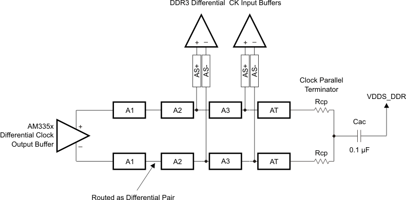 Figure 7-52 CK Topology for Two DDR3 Devices
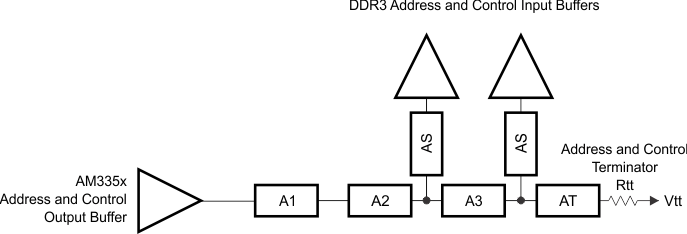 Figure 7-53 ADDR_CTRL Topology for Two DDR3 Devices
7.7.2.3.4.1.2 CK and ADDR_CTRL Routing, Two DDR3 Devices
Figure 7-54 shows the CK routing for two DDR3 devices placed on the same side of the PCB. Figure 7-55 shows the corresponding ADDR_CTRL routing.
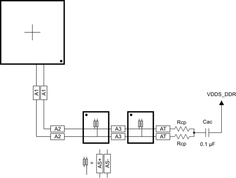 Figure 7-54 CK Routing for Two Single-Sided DDR3 Devices
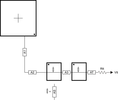 Figure 7-55 ADDR_CTRL Routing for Two Single-Sided DDR3 Devices
To save PCB space, the two DDR3 memories may be mounted as a mirrored pair at a cost of increased routing and assembly complexity. Figure 7-56 and Figure 7-57 show the routing for CK and ADDR_CTRL, respectively, for two DDR3 devices mirrored in a single-pair configuration.
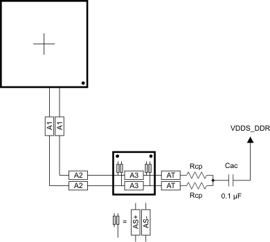 Figure 7-56 CK Routing for Two Mirrored DDR3 Devices
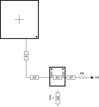 Figure 7-57 ADDR_CTRL Routing for Two Mirrored DDR3 Devices
7.7.2.3.4.2 One DDR3 Device
One DDR3 device is supported on the DDR3 interface consisting of one x16 DDR3 device arranged as one 16-bit bank.
7.7.2.3.4.2.1 CK and ADDR_CTRL Topologies, One DDR3 Device
Figure 7-58 shows the topology of the CK net classes and Figure 7-59 shows the topology for the corresponding ADDR_CTRL net classes.
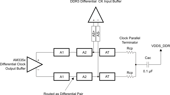 Figure 7-58 CK Topology for One DDR3 Device
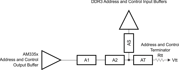 Figure 7-59 ADDR_CTRL Topology for One DDR3 Device
7.7.2.3.4.2.2 CK and ADDR_CTRL Routing, One DDR3 Device
Figure 7-60 shows the CK routing for one DDR3 device. Figure 7-61 shows the corresponding ADDR_CTRL routing.
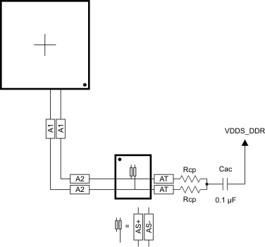 Figure 7-60 CK Routing for One DDR3 Device
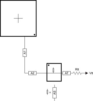 Figure 7-61 ADDR_CTRL Routing for One DDR3 Device
7.7.2.3.5 Data Topologies and Routing Definition
No matter the number of DDR3 devices used, the data line topology is always point to point, so its definition is simple.
7.7.2.3.5.1 DQS[x] and DQ[x] Topologies, Any Number of Allowed DDR3 Devices
DQS[x] lines are point-to-point differential, and DQ[x] lines are point-to-point single-ended. Figure 7-62 and Figure 7-63 show these topologies.
![AM3359 AM3358 AM3357 AM3356 AM3354 AM3352 AM3351 DQS[x]
Topology AM3359 AM3358 AM3357 AM3356 AM3354 AM3352 AM3351 dqs_topo_sprs717.gif](/ods/images/JAJSDZ0J/dqs_topo_sprs717.gif)
![AM3359 AM3358 AM3357 AM3356 AM3354 AM3352 AM3351 DQ[x]
Topology AM3359 AM3358 AM3357 AM3356 AM3354 AM3352 AM3351 dq_dm_topo_sprs717.gif](/ods/images/JAJSDZ0J/dq_dm_topo_sprs717.gif)
7.7.2.3.5.2 DQS[x] and DQ[x] Routing, Any Number of Allowed DDR3 Devices
Figure 7-64 and Figure 7-65 show the DQS[x] and DQ[x] routing.
![AM3359 AM3358 AM3357 AM3356 AM3354 AM3352 AM3351 DQS[x] Routing With
Any Number of Allowed DDR3 Devices AM3359 AM3358 AM3357 AM3356 AM3354 AM3352 AM3351 dqs_routing_sprs717.gif](/ods/images/JAJSDZ0J/dqs_routing_sprs717.gif)
![AM3359 AM3358 AM3357 AM3356 AM3354 AM3352 AM3351 DQ[x] Routing With
Any Number of Allowed DDR3 Devices AM3359 AM3358 AM3357 AM3356 AM3354 AM3352 AM3351 dq_dm_routing_sprs717.gif](/ods/images/JAJSDZ0J/dq_dm_routing_sprs717.gif)
7.7.2.3.6 Routing Specification
7.7.2.3.6.1 CK and ADDR_CTRL Routing Specification
Skew within the CK and ADDR_CTRL net classes directly reduces setup and hold margin and, thus, this skew must be controlled. The only way to practically match lengths on a PCB is to lengthen the shorter traces up to the length of the longest net in the net class and its associated clock. A metric to establish this maximum length is Manhattan distance. The Manhattan distance between two points on a PCB is the length between the points when connecting them only with horizontal or vertical segments. A reasonable trace route length is to within a percentage of its Manhattan distance. CACLM is defined as Clock Address Control Longest Manhattan distance.
Given the clock and address pin locations on the AM335x device and the DDR3 memories, the maximum possible Manhattan distance can be determined given the placement. Figure 7-66 shows this distance for two loads. The specifications on the lengths of the transmission lines for the address bus are determined from this distance. CACLM is determined similarly for other address bus configurations; that is, it is based on the longest net of the CK and ADDR_CTRL net class. For CK and ADDR_CTRL routing, these specifications are contained in Table 7-66.
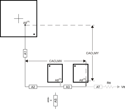
The length of shorter CK and ADDR_CTRL stubs as well as the length of the terminator stub are not included in this length calculation. Nonincluded lengths are grayed out in the figure.
Assuming A8 is the longest, CALM = CACLMY + CACLMX + 300 mils.
The extra 300 mils allows for routing down lower than the DDR3 memories and returning up to reach A8.
Table 7-66 CK and ADDR_CTRL Routing Specification(1)(2)(3)
| NO. | PARAMETER | MIN | TYP | MAX | UNIT |
|---|---|---|---|---|---|
| 1 | A1 + A2 length | 2500 | mils | ||
| 2 | A1 + A2 skew | 25 | mils | ||
| 3 | A3 length | 660 | mils | ||
| 4 | A3 skew(4) | 25 | mils | ||
| 5 | A3 skew(5) | 125 | mils | ||
| 6 | AS length | 100 | mils | ||
| 7 | AS skew | 25 | mils | ||
| 8 | AS+ and AS– length | 70 | mils | ||
| 9 | AS+ and AS– skew | 5 | mils | ||
| 10 | AT length(6) | 500 | mils | ||
| 11 | AT skew(7) | 100 | mils | ||
| 12 | AT skew(8) | 5 | mils | ||
| 13 | CK and ADDR_CTRL nominal trace length(9) | CACLM-50 | CACLM | CACLM+50 | mils |
| 14 | Center-to-center CK to other DDR3 trace spacing(10) | 4w | |||
| 15 | Center-to-center ADDR_CTRL to other DDR3 trace spacing(10)(11) | 4w | |||
| 16 | Center-to-center ADDR_CTRL to other ADDR_CTRL trace spacing(10) | 3w | |||
| 17 | CK center-to-center spacing(12) | ||||
| 18 | CK spacing to other net(10) | 4w | |||
| 19 | Rcp(13) | Zo-1 | Zo | Zo+1 | Ω |
| 20 | Rtt(13)(14) | Zo-5 | Zo | Zo+5 | Ω |
- CK represents the clock net class, and ADDR_CTRL represents the address and control signal net class.
- The use of vias should be minimized.
- Additional bypass capacitors are required when using the VDDS_DDR plane as the reference plane to allow the return current to jump between the VDDS_DDR plane and the ground plane when the net class switches layers at a via.
- Mirrored configuration (one DDR3 device on top of the board and one DDR3 device on the bottom).
- Nonmirrored configuration (all DDR3 memories on same side of PCB).
- While this length can be increased for convenience, its length should be minimized.
- ADDR_CTRL net class only (not CK net class). Minimizing this skew is recommended, but not required.
- CK net class only.
- CACLM is the longest Manhattan distance of the CK and ADDR_CTRL net classes + 300 mils. For definition, see Section 7.7.2.3.6.1 and Figure 7-66.
- Center-to-center spacing is allowed to fall to minimum (w) for up to 1250 mils of routed length.
- Signals from one DQ net class should be considered other DDR3 traces to another DQ net class.
- CK spacing set to ensure proper differential impedance. Differential impedance should be Zo x 2, where Zo is the single-ended impedance defined in Table 7-60.
- Source termination (series resistor at driver) is specifically not allowed.
- Termination values should be uniform across the net class.
7.7.2.3.6.2 DQS[x] and DQ[x] Routing Specification
Skew within the DQS[x] and DQ[x] net classes directly reduces setup and hold margin and, thus, this skew must be controlled. The only way to practically match lengths on a PCB is to lengthen the shorter traces up to the length of the longest net in the net class and its associated clock. DQLMn is defined as DQ Longest Manhattan distance n, where n is the byte number. For a 16-bit interface, there are two DQLMs, DQLM0-DQLM1.
NOTE
Matching the lengths across all bytes is not required, nor is it recommended. Length matching is only required within each byte.
Given the DQS[x] and DQ[x] pin locations on the AM335x device and the DDR3 memories, the maximum possible Manhattan distance can be determined given the placement. Figure 7-67 shows this distance for a two-load case. It is from this distance that the specifications on the lengths of the transmission lines for the data bus are determined. For DQS[x] and DQ[x] routing, these specifications are contained in Table 7-67.
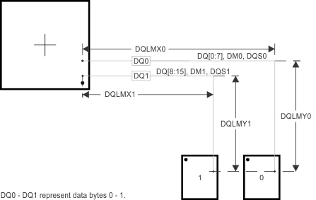
DQLM0 = DQLMX0 + DQLMY0
DQLM1 = DQLMX1 + DQLMY1
Table 7-67 DQS[x] and DQ[x] Routing Specification(1)(2)
| NO. | PARAMETER | MIN | TYP | MAX | UNIT |
|---|---|---|---|---|---|
| 1 | DQ0 nominal length(3)(4) | DQLM0 | mils | ||
| 2 | DQ1 nominal length(3)(5) | DQLM1 | mils | ||
| 3 | DQ[x] skew(6) | 25 | mils | ||
| 4 | DQS[x] skew | 5 | mils | ||
| 5 | DQS[x]-to-DQ[x] skew(6)(7) | 25 | mils | ||
| 6 | Center-to-center DQ[x] to other DDR3 trace spacing(8)(9) | 4w | |||
| 7 | Center-to-center DQ[x] to other DQ[x] trace spacing(8)(10) | 3w | |||
| 8 | DQS[x] center-to-center spacing(11) | ||||
| 9 | DQS[x] center-to-center spacing to other net(8) | 4w |
- DQS[x] represents the DQS0 and DQS1 clock net classes, and DQ[x] represents the DQ0 and DQ1 signal net classes.
- External termination disallowed. Data termination should use built-in ODT functionality.
- DQLMn is the longest Manhattan distance of a byte. For definition, see Section 7.7.2.3.6.2 and Figure 7-67.
- DQLM0 is the longest Manhattan length for the DQ0 net class.
- DQLM1 is the longest Manhattan length for the DQ1 net class.
- Length matching is only done within a byte. Length matching across bytes is not required.
- Each DQS clock net class is length matched to its associated DQ signal net class.
- Center-to-center spacing is allowed to fall to minimum for up to 1250 mils of routed length.
- Other DDR3 trace spacing means signals that are not part of the same DQ[x] signal net class.
- This applies to spacing within same DQ[x] signal net class.
- DQS[x] pair spacing is set to ensure proper differential impedance. Differential impedance should be Zo x 2, where Zo is the single-ended impedance defined in Table 7-60.
7.8 I2C
For more information, see the Inter-Integrated Circuit (I2C) section of the AM335x and AMIC110 Sitara Processors Technical Reference Manual.
7.8.1 I2C Electrical Data and Timing
Table 7-68 I2C Timing Conditions – Slave Mode
| PARAMETER | STANDARD MODE | FAST MODE | UNIT | |||
|---|---|---|---|---|---|---|
| MIN | MAX | MIN | MAX | |||
| Output Condition | ||||||
| Cb | Capacitive load for each bus line | 400 | 400 | pF | ||
Table 7-69 Timing Requirements for I2C Input Timings
(see Figure 7-68)| NO. | STANDARD MODE | FAST MODE | UNIT | ||||
|---|---|---|---|---|---|---|---|
| MIN | MAX | MIN | MAX | ||||
| 1 | tc(SCL) | Cycle time, SCL | 10 | 2.5 | µs | ||
| 2 | tsu(SCLH-SDAL) | Setup time, SCL high before SDA low (for a repeated START condition) | 4.7 | 0.6 | µs | ||
| 3 | th(SDAL-SCLL) | Hold time, SCL low after SDA low (for a START and a repeated START condition) | 4 | 0.6 | µs | ||
| 4 | tw(SCLL) | Pulse duration, SCL low | 4.7 | 1.3 | µs | ||
| 5 | tw(SCLH) | Pulse duration, SCL high | 4 | 0.6 | µs | ||
| 6 | tsu(SDAV-SCLH) | Setup time, SDA valid before SCL high | 250 | 100(1) | ns | ||
| 7 | th(SCLL-SDAV) | Hold time, SDA valid after SCL low | 0(2) | 3.45(3) | 0(2) | 0.9(3) | µs |
| 8 | tw(SDAH) | Pulse duration, SDA high between STOP and START conditions | 4.7 | 1.3 | µs | ||
| 9 | tr(SDA) | Rise time, SDA | 1000 | 300 | ns | ||
| 10 | tr(SCL) | Rise time, SCL | 1000 | 300 | ns | ||
| 11 | tf(SDA) | Fall time, SDA | 300 | 300 | ns | ||
| 12 | tf(SCL) | Fall time, SCL | 300 | 300 | ns | ||
| 13 | tsu(SCLH-SDAH) | Setup time, high before SDA high (for STOP condition) | 4 | 0.6 | µs | ||
| 14 | tw(SP) | Pulse duration, spike (must be suppressed) | 0 | 50 | 0 | 50 | ns |
- A fast-mode I2C-bus device can be used in a standard-mode I2C-bus system, but the requirement tsu(SDA-SCLH)≥ 250 ns must then be met. This is automatically the case if the device does not stretch the LOW period of the SCL signal. If such a device stretches the LOW period of the SCL signal, it must output the next data bit to the SDA line tr max + tsu(SDA-SCLH) = 1000 + 250 = 1250 ns (according to the standard-mode I2C-Bus Specification) before the SCL line is released.
- A device must internally provide a hold time of at least 300 ns for the SDA signal (referred to the VIHmin of the SCL signal) to bridge the undefined region of the falling edge of SCL.
- The maximum th(SDA-SCLL) has only to be met if the device does not stretch the low period [tw(SCLL)] of the SCL signal.
 Figure 7-68 I2C Receive Timing
Table 7-70 Switching Characteristics for I2C Output Timings
(see Figure 7-69)| NO. | PARAMETER | STANDARD MODE | FAST MODE | UNIT | |||
|---|---|---|---|---|---|---|---|
| MIN | MAX | MIN | MAX | ||||
| 15 | tc(SCL) | Cycle time, SCL | 10 | 2.5 | µs | ||
| 16 | tsu(SCLH-SDAL) | Setup time, SCL high before SDA low (for a repeated START condition) | 4.7 | 0.6 | µs | ||
| 17 | th(SDAL-SCLL) | Hold time, SCL low after SDA low (for a START and a repeated START condition) | 4 | 0.6 | µs | ||
| 18 | tw(SCLL) | Pulse duration, SCL low | 4.7 | 1.3 | µs | ||
| 19 | tw(SCLH) | Pulse duration, SCL high | 4 | 0.6 | µs | ||
| 20 | tsu(SDAV-SCLH) | Setup time, SDA valid before SCL high | 250 | 100 | ns | ||
| 21 | th(SCLL-SDAV) | Hold time, SDA valid after SCL low | 0 | 3.45 | 0 | 0.9 | µs |
| 22 | tw(SDAH) | Pulse duration, SDA high between STOP and START conditions | 4.7 | 1.3 | µs | ||
| 23 | tr(SDA) | Rise time, SDA | 1000 | 300 | ns | ||
| 24 | tr(SCL) | Rise time, SCL | 1000 | 300 | ns | ||
| 25 | tf(SDA) | Fall time, SDA | 300 | 300 | ns | ||
| 26 | tf(SCL) | Fall time, SCL | 300 | 300 | ns | ||
| 27 | tsu(SCLH-SDAH) | Setup time, high before SDA high (for STOP condition) | 4 | 0.6 | µs | ||
7.9 JTAG Electrical Data and Timing
Table 7-71 Timing Requirements for JTAG
(see Figure 7-70)| NO. | OPP100 | OPP50 | UNIT | ||||
|---|---|---|---|---|---|---|---|
| MIN | MAX | MIN | MAX | ||||
| 1 | tc(TCK) | Cycle time, TCK | 81.5 | 104.5 | ns | ||
| 1a | tw(TCKH) | Pulse duration, TCK high (40% of tc) | 32.6 | 41.8 | ns | ||
| 1b | tw(TCKL) | Pulse duration, TCK low (40% of tc) | 32.6 | 41.8 | ns | ||
| 3 | tsu(TDI-TCKH) | Input setup time, TDI valid to TCK high | 3 | 3 | ns | ||
| tsu(TMS-TCKH) | Input setup time, TMS valid to TCK high | 3 | 3 | ns | |||
| 4 | th(TCKH-TDI) | Input hold time, TDI valid from TCK high | 8.05 | 8.05 | ns | ||
| th(TCKH-TMS) | Input hold time, TMS valid from TCK high | 8.05 | 8.05 | ns | |||
Table 7-72 Switching Characteristics for JTAG
(see Figure 7-70)| NO. | PARAMETER | OPP100 | OPP50 | UNIT | |||
|---|---|---|---|---|---|---|---|
| MIN | MAX | MIN | MAX | ||||
| 2 | td(TCKL-TDO) | Delay time, TCK low to TDO valid | 3 | 27.6 | 4 | 36.8 | ns |
 Figure 7-70 JTAG Timing
7.10 LCD Controller (LCDC)
The LCDC consists of two independent controllers, the raster controller and the LCD interface display driver (LIDD) controller. Each controller operates independently from the other and only one of them is active at any given time.
- The raster controller handles the synchronous LCD interface. It provides timing and data for constant graphics refresh to a passive display. It supports a wide variety of monochrome and full-color display types and sizes by use of programmable timing controls, a built-in palette, and a gray-scale and serializer. Graphics data is processed and stored in frame buffers. A frame buffer is a contiguous memory block in the system. A built-in DMA engine supplies the graphics data to the raster engine which, in turn, outputs to the external LCD device.
- The LIDD controller supports the asynchronous LCD interface. It provides full-timing programmability of control signals (CS, WE, OE, ALE) and output data.
The maximum resolution for the LCD controller is 2048 × 2048 pixels. The maximum frame rate is determined by the image size in combination with the pixel clock rate.
Table 7-73 LCD Controller Timing Conditions
| PARAMETER | MIN | TYP | MAX | UNIT | ||
|---|---|---|---|---|---|---|
| Output Condition | ||||||
| CLOAD | Output load capacitance | LIDD mode | 5 | 60 | pF | |
| Raster mode | 3 | 30 | ||||
7.10.1 LCD Interface Display Driver (LIDD Mode)
Table 7-74 Timing Requirements for LCD LIDD Mode
(see Figure 7-72 through Figure 7-80)| NO. | OPP100 | UNIT | |||
|---|---|---|---|---|---|
| MIN | MAX | ||||
| 16 | tsu(LCD_DATA-LCD_MEMORY_CLK) | Setup time, LCD_DATA[15:0] valid before LCD_MEMORY_CLK high | 18 | ns | |
| 17 | th(LCD_MEMORY_CLK-LCD_DATA) | Hold time, LCD_DATA[15:0] valid after LCD_MEMORY_CLK high | 0 | ns | |
| 18 | tt(LCD_DATA) | Transition time, LCD_DATA[15:0] | 1 | 3 | ns |
Table 7-75 Switching Characteristics for LCD LIDD Mode
(see Figure 7-72 through Figure 7-80)| NO. | PARAMETER | OPP100 | UNIT | ||
|---|---|---|---|---|---|
| MIN | MAX | ||||
| 1 | tc(LCD_MEMORY_CLK) | Cycle time, LCD_MEMORY_CLK | 23.7 | ns | |
| 2 | tw(LCD_MEMORY_CLKH) | Pulse duration, LCD_MEMORY_CLK high | 0.45tc | 0.55tc | ns |
| 3 | tw(LCD_MEMORY_CLKL) | Pulse duration, LCD_MEMORY_CLK low | 0.45tc | 0.55tc | ns |
| 4 | td(LCD_MEMORY_CLK-LCD_DATAV) | Delay time, LCD_MEMORY_CLK high to LCD_DATA[15:0] valid (write) | 7 | ns | |
| 5 | td(LCD_MEMORY_CLK-LCD_DATAI) | Delay time, LCD_MEMORY_CLK high to LCD_DATA[15:0] invalid (write) | 0 | ns | |
| 6 | td(LCD_MEMORY_CLK-LCD_AC_BIAS_EN) | Delay time, LCD_MEMORY_CLK high to LCD_AC_BIAS_EN | 0 | 6.8 | ns |
| 7 | tt(LCD_AC_BIAS_EN) | Transition time, LCD_AC_BIAS_EN | 1 | 10 | ns |
| 8 | td(LCD_MEMORY_CLK-LCD_VSYNC) | Delay time, LCD_MEMORY_CLK high to LCD_VSYNC | 0 | 7 | ns |
| 9 | tt(LCD_VSYNC) | Transition time, LCD_VSYNC | 1 | 10 | ns |
| 10 | td(LCD_MEMORY_CLK-LCD_HYSNC) | Delay time, LCD_MEMORY_CLK high to LCD_HSYNC | 0 | 7 | ns |
| 11 | tt(LCD_HSYNC) | Transition time, LCD_HYSNC | 1 | 10 | ns |
| 12 | td(LCD_MEMORY_CLK-LCD_PCLK) | Delay time, LCD_MEMORY_CLK high to LCD_PCLK | 0 | 7 | ns |
| 13 | tt(LCD_PCLK) | Transition time, LCD_PCLK | 1 | 10 | ns |
| 14 | td(LCD_MEMORY_CLK-LCD_DATAZ) | Delay time, LCD_MEMORY_CLK high to LCD_DATA[15:0] high-Z | 0 | 7 | ns |
| 15 | td(LCD_MEMORY_CLK-LCD_DATA) | Delay time, LCD_MEMORY_CLK high to LCD_DATA[15:0] driven | 0 | 7 | ns |
| 19 | tt(LCD_MEMORY_CLK) | Transition time, LCD_MEMORY_CLK | 1 | 2.5 | ns |
| 20 | tt(LCD_DATA) | Transition time, LCD_DATA | 1 | 10 | ns |
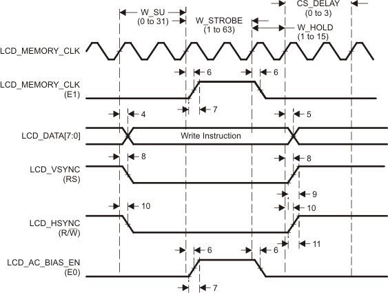
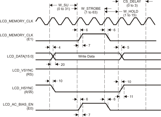
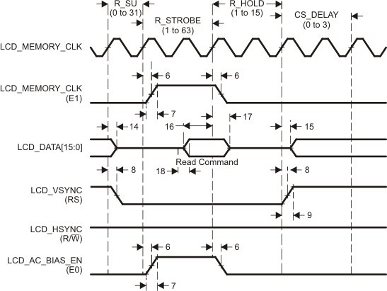
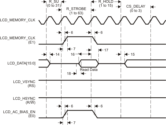
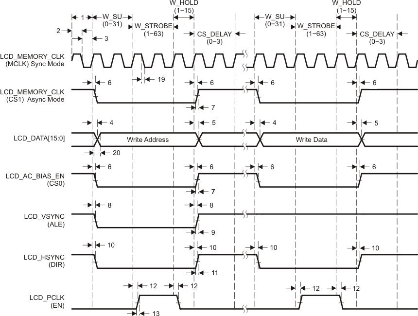
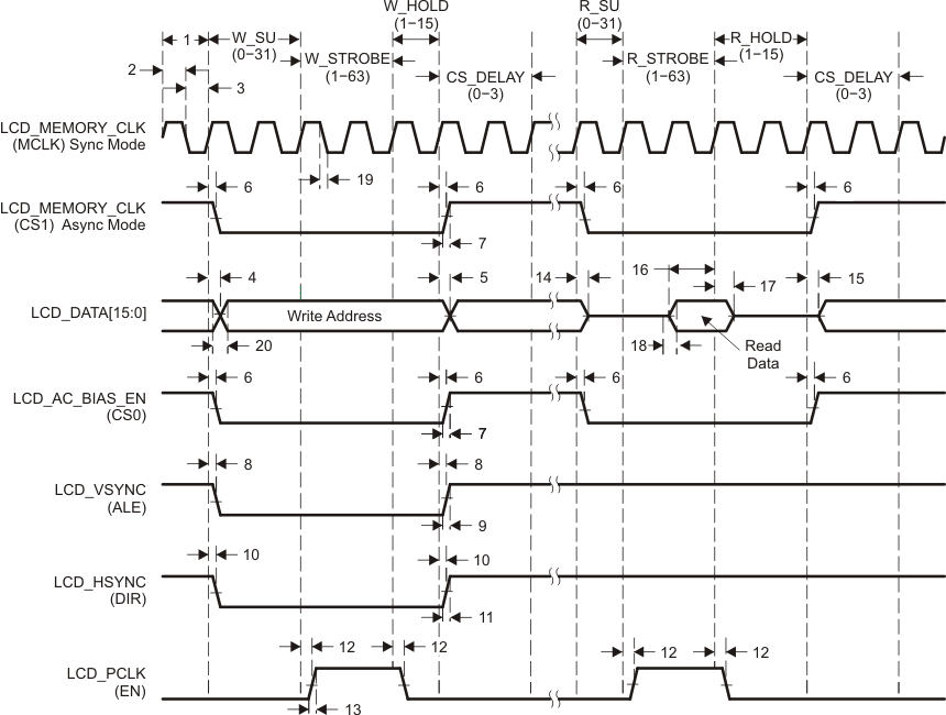
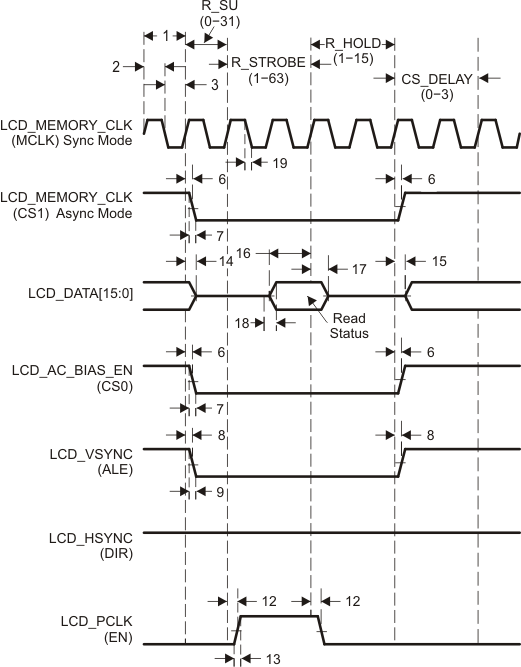
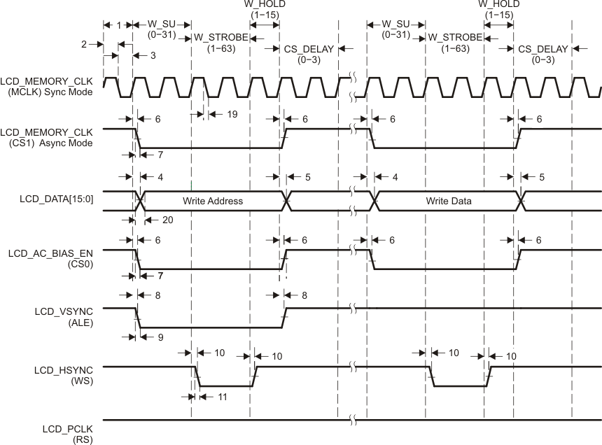
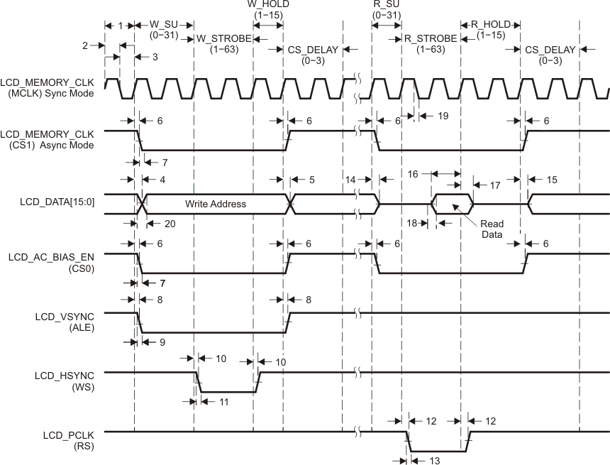
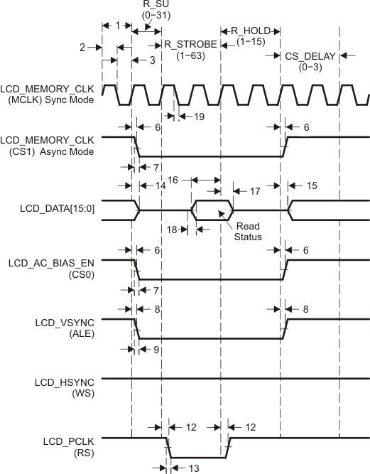
7.10.2 LCD Raster Mode
Table 7-76 Switching Characteristics for LCD Raster Mode
(see Figure 7-82 through Figure 7-85)| NO. | PARAMETER | OPP50 | OPP100 | UNIT | |||
|---|---|---|---|---|---|---|---|
| MIN | MAX | MIN | MAX | ||||
| 1 | tc(LCD_PCLK) | Cycle time, pixel clock | 15.8 | 7.9 | ns | ||
| 2 | tw(LCD_PCLKH) | Pulse duration, pixel clock high | 0.45tc | 0.55tc | 0.45tc | 0.55tc | ns |
| 3 | tw(LCD_PCLKL) | Pulse duration, pixel clock low | 0.45tc | 0.55tc | 0.45tc | 0.55tc | ns |
| 4 | td(LCD_PCLK-LCD_DATAV) | Delay time, LCD_PCLK to LCD_DATA[23:0] valid (write) | 3.0 | 1.9 | ns | ||
| 5 | td(LCD_PCLK-LCD_DATAI) | Delay time, LCD_PCLK to LCD_DATA[23:0] invalid (write) | –3.0 | –1.7 | ns | ||
| 6 | td(LCD_PCLK-LCD_AC_BIAS_EN) | Delay time, LCD_PCLK to LCD_AC_BIAS_EN | –3.0 | 3.0 | –1.7 | 1.9 | ns |
| 7 | tt(LCD_AC_BIAS_EN) | Transition time, LCD_AC_BIAS_EN | 0.5 | 2.4 | 0.5 | 2.4 | ns |
| 8 | td(LCD_PCLK-LCD_VSYNC) | Delay time, LCD_PCLK to LCD_VSYNC | –3.0 | 3.0 | –1.7 | 1.9 | ns |
| 9 | tt(LCD_VSYNC) | Transition time, LCD_VSYNC | 0.5 | 2.4 | 0.5 | 2.4 | ns |
| 10 | td(LCD_PCLK-LCD_HSYNC) | Delay time, LCD_PCLK to LCD_HSYNC | –3.0 | 3.0 | –1.7 | 1.9 | ns |
| 11 | tt(LCD_HSYNC) | Transition time, LCD_HSYNC | 0.5 | 2.4 | 0.5 | 2.4 | ns |
| 12 | tt(LCD_PCLK) | Transition time, LCD_PCLK | 0.5 | 2.4 | 0.5 | 2.4 | ns |
| 13 | tt(LCD_DATA) | Transition time, LCD_DATA | 0.5 | 2.4 | 0.5 | 2.4 | ns |
Frame-to-frame timing is derived through the following parameters in the LCD (RASTER_TIMING_1) register:
- Vertical front porch (VFP)
- Vertical sync pulse width (VSW)
- Vertical back porch (VBP)
- Lines per panel (LPP_B10 + LPP)
Line-to-line timing is derived through the following parameters in the LCD (RASTER_TIMING_0) register:
- Horizontal front porch (HFP)
- Horizontal sync pulse width (HSW)
- Horizontal back porch (HBP)
- Pixels per panel (PPLMSB + PPLLSB)
LCD_AC_BIAS_EN timing is derived through the following parameter in the LCD (RASTER_TIMING_2) register:
- AC bias frequency (ACB)
The display format produced in raster mode is shown in Figure 7-81. An entire frame is delivered one line at a time. The first line delivered starts at data pixel (1, 1) and ends at data pixel (P, 1). The last line delivered starts at data pixel (1, L) and ends at data pixel (P, L). The beginning of each new frame is denoted by the activation of I/O signal LCD_VSYNC. The beginning of each new line is denoted by the activation of I/O signal LCD_HSYNC.
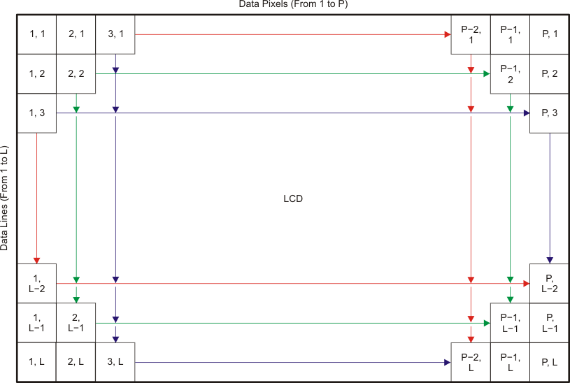 Figure 7-81 LCD Raster-Mode Display Format
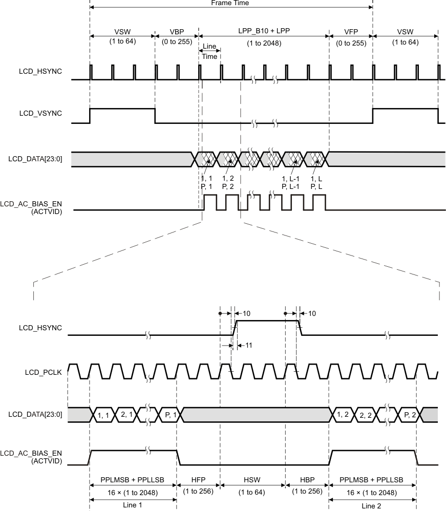 Figure 7-82 LCD Raster-Mode Active
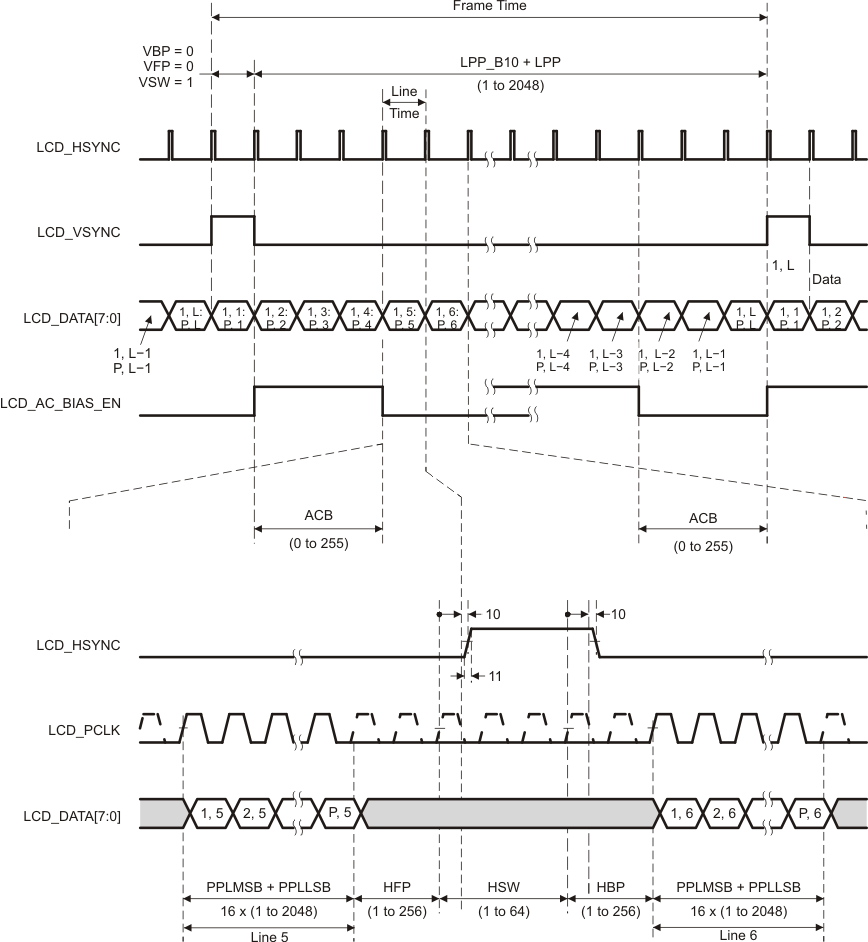
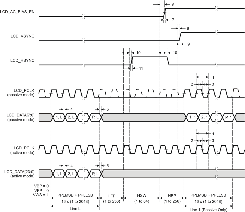
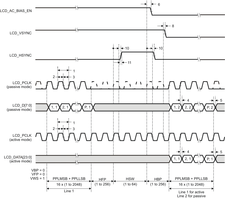
7.11 Multichannel Audio Serial Port (McASP)
The multichannel audio serial port (McASP) functions as a general-purpose audio serial port optimized for the needs of multichannel audio applications. The McASP is useful for time-division multiplexed (TDM) stream, Inter-Integrated Sound (I2S) protocols, and inter-component digital audio interface transmission (DIT).
7.11.1 McASP Device-Specific Information
The device includes two multichannel audio serial port (McASP) interface peripherals (McASP0 and McASP1). The McASP module consists of a transmit and receive section. These sections can operate completely independently with different data formats, separate master clocks, bit clocks, and frame syncs or, alternatively, the transmit and receive sections may be synchronized. The McASP module also includes shift registers that may be configured to operate as either transmit data or receive data.
The transmit section of the McASP can transmit data in either a time-division-multiplexed (TDM) synchronous serial format or in a digital audio interface (DIT) format where the bit stream is encoded for SPDIF, AES-3, IEC-60958, CP-430 transmission. The receive section of the McASP peripheral supports the TDM synchronous serial format.
The McASP module can support one transmit data format (either a TDM format or DIT format) and one receive format at a time. All transmit shift registers use the same format and all receive shift registers use the same format; however, the transmit and receive formats need not be the same. Both the transmit and receive sections of the McASP also support burst mode, which is useful for nonaudio data (for example, passing control information between two devices).
The McASP peripheral has additional capability for flexible clock generation and error detection/handling, as well as error management.
The device McASP0 and McASP1 modules have up to four serial data pins each. The McASP FIFO size is 256 bytes and two DMA and two interrupt requests are supported. Buffers are used transparently to better manage DMA, which can be leveraged to manage data flow more efficiently.
For more detailed information on and the functionality of the McASP peripheral, see the Multichannel Audio Serial Port (McASP) section of the AM335x and AMIC110 Sitara Processors Technical Reference Manual.
7.11.2 McASP Electrical Data and Timing
Table 7-77 McASP Timing Conditions
| PARAMETER | MIN | TYP | MAX | UNIT | |
|---|---|---|---|---|---|
| Input Conditions | |||||
| tR | Input signal rise time | 1(1) | 4(1) | ns | |
| tF | Input signal fall time | 1(1) | 4(1) | ns | |
| Output Condition | |||||
| CLOAD | Output load capacitance | 15 | 30 | pF | |
- Except when specified otherwise.
Table 7-78 Timing Requirements for McASP(1)
(see Figure 7-86)| NO. | OPP100 | OPP50 | UNIT | |||||
|---|---|---|---|---|---|---|---|---|
| MIN | MAX | MIN | MAX | |||||
| 1 | tc(AHCLKRX) | Cycle time, McASP[x]_AHCLKR and McASP[x]_AHCLKX | 20 | 40 | ns | |||
| 2 | tw(AHCLKRX) | Pulse duration, McASP[x]_AHCLKR and McASP[x]_AHCLKX high or low | 0.5P - 2.5(2) | 0.5P - 2.5(2) | ns | |||
| 3 | tc(ACLKRX) | Cycle time, McASP[x]_ACLKR and McASP[x]_ACLKX | 20 | 40 | ns | |||
| 4 | tw(ACLKRX) | Pulse duration, McASP[x]_ACLKR and McASP[x]_ACLKX high or low | 0.5R - 2.5(3) | 0.5R - 2.5(3) | ns | |||
| 5 | tsu(AFSRX-ACLKRX) | Setup time, McASP[x]_AFSR and McASP[x]_AFSX input valid before McASP[x]_ACLKR and McASP[x]_ACLKX | ACLKR and ACLKX int | 11.5 | 15.5 | ns | ||
| ACLKR and ACLKX ext in | 4 | 6 | ||||||
| ACLKR and ACLKX ext out | 4 | 6 | ||||||
| 6 | th(ACLKRX-AFSRX) | Hold time, McASP[x]_AFSR and McASP[x]_AFSX input valid after McASP[x]_ACLKR and McASP[x]_ACLKX | ACLKR and ACLKX int | -1 | -1 | ns | ||
| ACLKR and ACLKX ext in | 0.4 | 0.4 | ||||||
| ACLKR and ACLKX ext out | 0.4 | 0.4 | ||||||
| 7 | tsu(AXR-ACLKRX) | Setup time, McASP[x]_AXR input valid before McASP[x]_ACLKR and McASP[x]_ACLKX | ACLKR and ACLKX int | 11.5 | 15.5 | ns | ||
| ACLKR and ACLKX ext in | 4 | 6 | ||||||
| ACLKR and ACLKX ext out | 4 | 6 | ||||||
| 8 | th(ACLKRX-AXR) | Hold time, McASP[x]_AXR input valid after McASP[x]_ACLKR and McASP[x]_ACLKX | ACLKR and ACLKX int | -1 | -1 | ns | ||
| ACLKR and ACLKX ext in | 0.4 | 0.4 | ||||||
| ACLKR and ACLKX ext out | 0.4 | 0.4 | ||||||
- ACLKR internal: ACLKRCTL.CLKRM = 1, PDIR.ACLKR = 1
ACLKR external input: ACLKRCTL.CLKRM = 0, PDIR.ACLKR = 0
ACLKR external output: ACLKRCTL.CLKRM = 0, PDIR.ACLKR = 1
ACLKX internal: ACLKXCTL.CLKXM = 1, PDIR.ACLKX = 1
ACLKX external input: ACLKXCTL.CLKXM = 0, PDIR.ACLKX = 0
ACLKX external output: ACLKXCTL.CLKXM = 0, PDIR.ACLKX = 1 - P = McASP[x]_AHCLKR and McASP[x]_AHCLKX period in nanoseconds (ns).
- R = McASP[x]_ACLKR and McASP[x]_ACLKX period in ns.
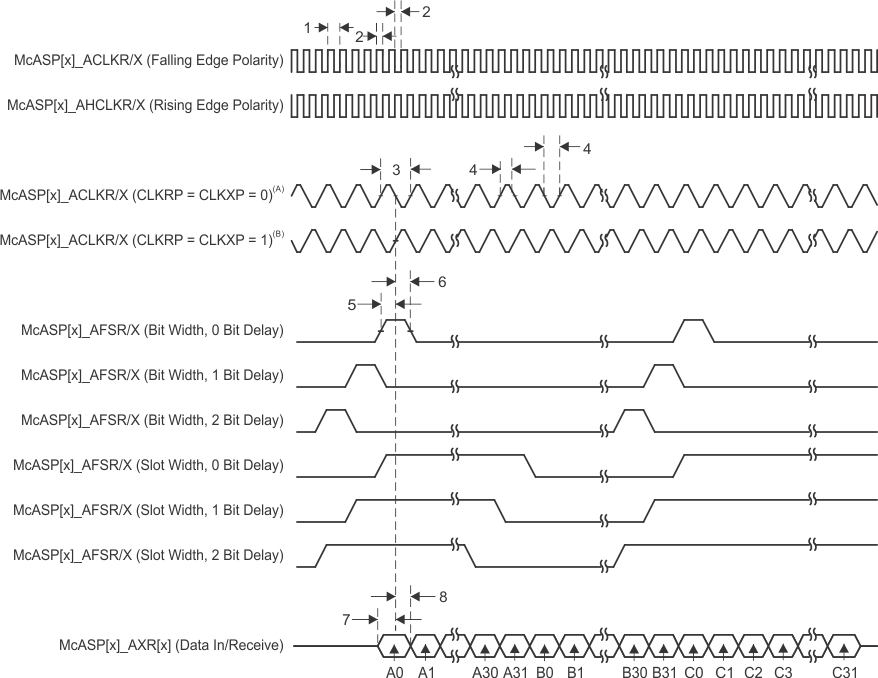
Table 7-79 Switching Characteristics for McASP(1)
(see Figure 7-87)| NO. | PARAMETER | OPP100 | OPP50 | UNIT | ||||
|---|---|---|---|---|---|---|---|---|
| MIN | MAX | MIN | MAX | |||||
| 9 | tc(AHCLKRX) | Cycle time, McASP[x]_AHCLKR and McASP[x]_AHCLKX | 20(2) | 40 | ns | |||
| 10 | tw(AHCLKRX) | Pulse duration, McASP[x]_AHCLKR and McASP[x]_AHCLKX high or low | 0.5P – 2.5(3) | 0.5P – 2.5(3) | ns | |||
| 11 | tc(ACLKRX) | Cycle time, McASP[x]_ACLKR and McASP[x]_ACLKX | 20 | 40 | ns | |||
| 12 | tw(ACLKRX) | Pulse duration, McASP[x]_ACLKR and McASP[x]_ACLKX high or low | 0.5P – 2.5(3) | 0.5P – 2.5(3) | ns | |||
| 13 | td(ACLKRX-AFSRX) | Delay time, McASP[x]_ACLKR and McASP[x]_ACLKX transmit edge to McASP[x]_AFSR and McASP[x]_AFSX output valid | ACLKR and ACLKX int | 0 | 6 | 0 | 6 | ns |
| ACLKR and ACLKX ext in | 2 | 13.5 | 2 | 18 | ||||
| Delay time, McASP[x]_ACLKR and McASP[x]_ACLKX transmit edge to McASP[x]_AFSR and McASP[x]_AFSX output valid with Pad Loopback | ACLKR and ACLKX ext out | 2 | 13.5 | 2 | 18 | |||
| 14 | td(ACLKX-AXR) | Delay time, McASP[x]_ACLKX transmit edge to McASP[x]_AXR output valid | ACLKX int | 0 | 6 | 0 | 6 | ns |
| ACLKX ext in | 2 | 13.5 | 2 | 18 | ||||
| Delay time, McASP[x]_ACLKX transmit edge to McASP[x]_AXR output valid with Pad Loopback | ACLKX ext out | 2 | 13.5 | 2 | 18 | |||
| 15 | tdis(ACLKX-AXR) | Disable time, McASP[x]_ACLKX transmit edge to McASP[x]_AXR output high impedance | ACLKX int | 0 | 6 | 0 | 6 | ns |
| ACLKX ext in | 2 | 13.5 | 2 | 18 | ||||
| Disable time, McASP[x]_ACLKX transmit edge to McASP[x]_AXR output high impedance with pad loopback | ACLKX ext out | 2 | 13.5 | 2 | 18 | |||
- ACLKR internal: ACLKRCTL.CLKRM = 1, PDIR.ACLKR = 1
ACLKR external input: ACLKRCTL.CLKRM = 0, PDIR.ACLKR = 0
ACLKR external output: ACLKRCTL.CLKRM = 0, PDIR.ACLKR = 1
ACLKX internal: ACLKXCTL.CLKXM = 1, PDIR.ACLKX = 1
ACLKX external input: ACLKXCTL.CLKXM = 0, PDIR.ACLKX = 0
ACLKX external output: ACLKXCTL.CLKXM = 0, PDIR.ACLKX = 1 - 50 MHz
- P = AHCLKR and AHCLKX period.
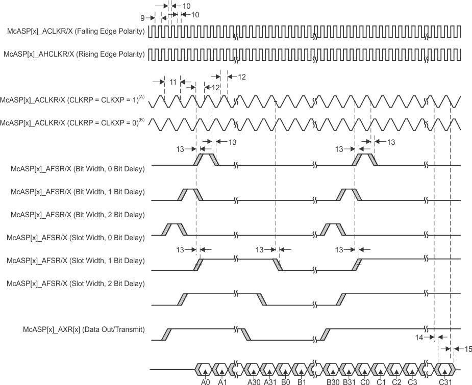
7.12 Multichannel Serial Port Interface (McSPI)
For more information, see the Multichannel Serial Port Interface (McSPI) section of the AM335x and AMIC110 Sitara Processors Technical Reference Manual.
7.12.1 McSPI Electrical Data and Timing
The following timings are applicable to the different configurations of McSPI in master or slave mode for any McSPI and any channel (n).
7.12.1.1 McSPI—Slave Mode
Table 7-80 McSPI Timing Conditions – Slave Mode
| PARAMETER | MIN | MAX | UNIT | |
|---|---|---|---|---|
| Input Conditions | ||||
| tr | Input signal rise time | 5 | ns | |
| tf | Input signal fall time | 5 | ns | |
| Output Condition | ||||
| Cload | Output load capacitance | 20 | pF | |
Table 7-81 Timing Requirements for McSPI Input Timings—Slave Mode
(see Figure 7-88)| NO. | OPP100 | OPP50 | UNIT | ||||
|---|---|---|---|---|---|---|---|
| MIN | MAX | MIN | MAX | ||||
| 1 | tc(SPICLK) | Cycle time, SPI_CLK | 62.5 | 124.8 | ns | ||
| 2 | tw(SPICLKL) | Typical pulse duration, SPI_CLK low | 0.5P – 3.12(1) | 0.5P + 3.12(1) | 0.5P – 3.12(1) | 0.5P + 3.12(1) | ns |
| 3 | tw(SPICLKH) | Typical pulse duration, SPI_CLK high | 0.5P – 3.12(1) | 0.5P + 3.12(1) | 0.5P – 3.12(1) | 0.5P + 3.12(1) | ns |
| 4 | tsu(SIMO-SPICLK) | Setup time, SPI_D[x] (SIMO) valid before SPI_CLK active edge(2)(3) | 12.92 | 12.92 | ns | ||
| 5 | th(SPICLK-SIMO) | Hold time, SPI_D[x] (SIMO) valid after SPI_CLK active edge(2)(3) | 12.92 | 12.92 | ns | ||
| 8 | tsu(CS-SPICLK) | Setup time, SPI_CS valid before SPI_CLK first edge(2) | 12.92 | 12.92 | ns | ||
| 9 | th(SPICLK-CS) | Hold time, SPI_CS valid after SPI_CLK last edge(2) | 12.92 | 12.92 | ns | ||
- P = SPI_CLK period.
- This timing applies to all configurations regardless of MCSPIX_CLK polarity and which clock edges are used to drive output data and capture input data.
- Pins SPIx_D0 and SPIx_D1 can function as SIMO or SOMI.
Table 7-82 Switching Characteristics for McSPI Output Timings—Slave Mode
(see Figure 7-89)| NO. | PARAMETER | OPP100 | OPP50 | UNIT | |||
|---|---|---|---|---|---|---|---|
| MIN | MAX | MIN | MAX | ||||
| 6 | td(SPICLK-SOMI) | Delay time, SPI_CLK active edge to SPI_D[x] (SOMI) transition(1)(2) | –4.00 | 17.12 | –4.00 | 17.12 | ns |
| 7 | td(CS-SOMI) | Delay time, SPI_CS active edge to SPI_D[x] (SOMI) transition(1)(2) | 17.12 | 17.12 | ns | ||
- This timing applies to all configurations regardless of MCSPIX_CLK polarity and which clock edges are used to drive output data and capture input data.
- Pins SPIx_D0 and SPIx_D1 can function as SIMO or SOMI.
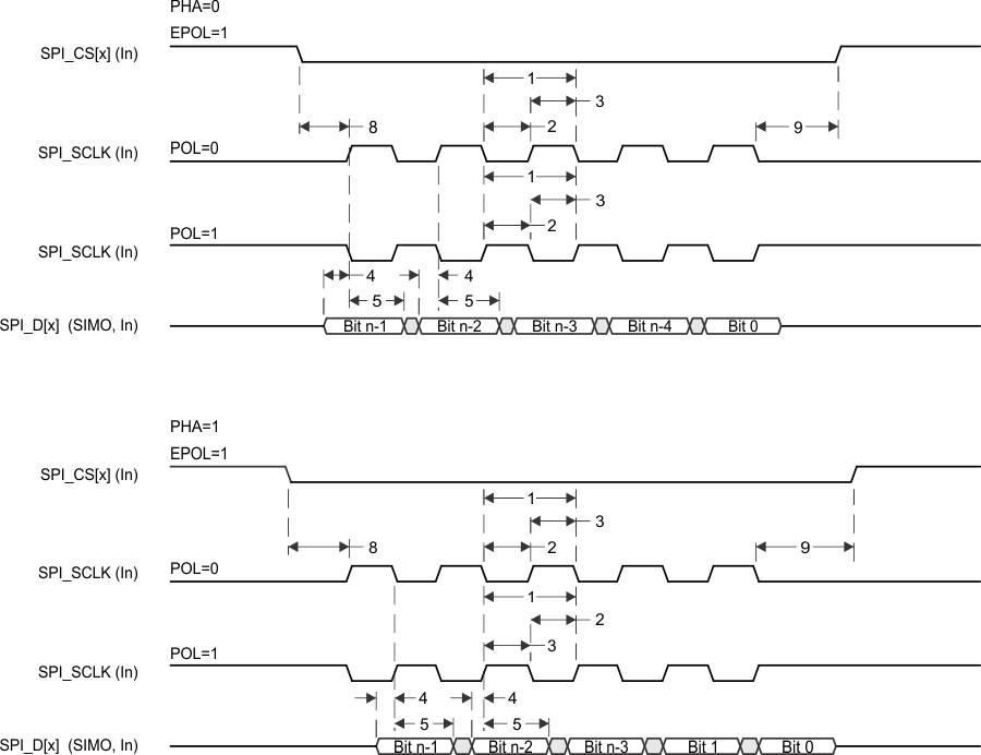 Figure 7-88 SPI Slave Mode Receive Timing
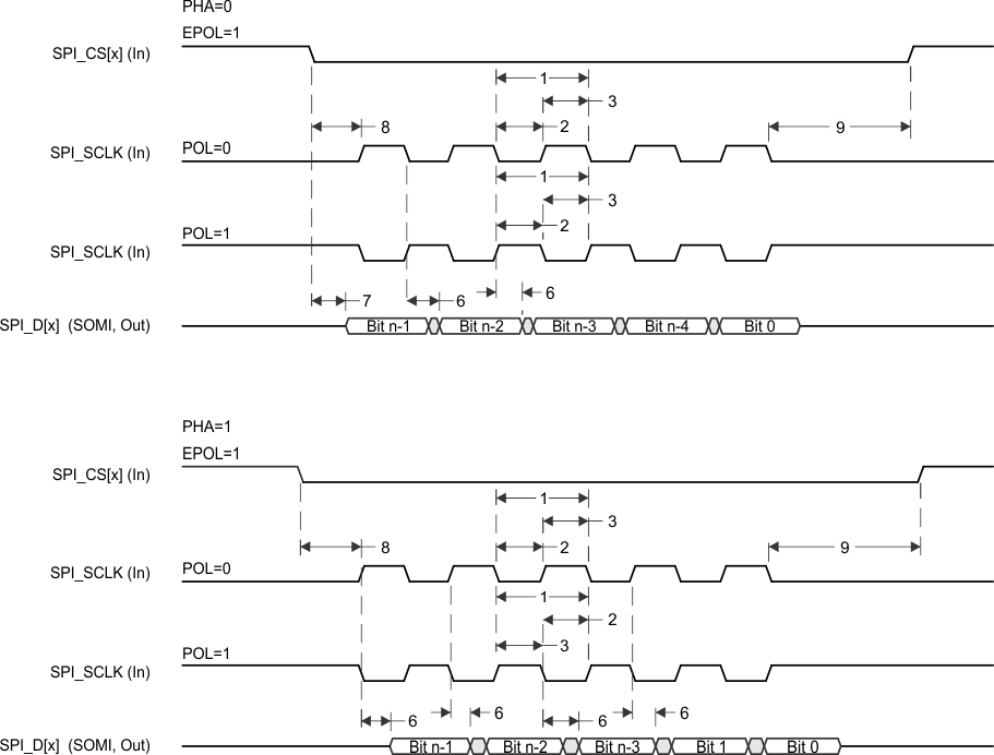 Figure 7-89 SPI Slave Mode Transmit Timing
7.12.1.2 McSPI—Master Mode
Table 7-83 McSPI Timing Conditions – Master Mode
| PARAMETER | LOW LOAD | HIGH LOAD | UNIT | |||
|---|---|---|---|---|---|---|
| MIN | MAX | MIN | MAX | |||
| Input Conditions | ||||||
| tr | Input signal rise time | 8 | 8 | ns | ||
| tf | Input signal fall time | 8 | 8 | ns | ||
| Output Condition | ||||||
| Cload | Output load capacitance | 5 | 25 | pF | ||
Table 7-84 Timing Requirements for McSPI Input Timings – Master Mode
(see Figure 7-90)| NO. | OPP100 | OPP50 | UNIT | |||||||||
|---|---|---|---|---|---|---|---|---|---|---|---|---|
| LOW LOAD | HIGH LOAD | LOW LOAD | HIGH LOAD | |||||||||
| MIN | MAX | MIN | MAX | MIN | MAX | MIN | MAX | |||||
| 4 | tsu(SOMI-SPICLKH) | Setup time, SPI_D[x] (SOMI) valid before SPI_CLK active edge(1) | 2.29 | 3.02 | 2.29 | 3.02 | ns | |||||
| 5 | th(SPICLKH-SOMI) | Hold time, SPI_D[x] (SOMI) valid after SPI_CLK active edge(1) | Industrial extended temperature (-40°C to 125°C) |
7.1 | 7.1 | 7.1 | 7.1 | ns | ||||
| All other temperature ranges | 4.7 | 4.7 | 4.7 | 4.7 | ||||||||
- Pins SPIx_D0 and SPIx_D1 can function as SIMO or SOMI.
Table 7-85 Switching Characteristics for McSPI Output Timings – Master Mode
(see Figure 7-91)| NO. | PARAMETER | OPP100 | OPP50 | UNIT | ||||||||
|---|---|---|---|---|---|---|---|---|---|---|---|---|
| LOW LOAD | HIGH LOAD | LOW LOAD | HIGH LOAD | |||||||||
| MIN | MAX | MIN | MAX | MIN | MAX | MIN | MAX | |||||
| 1 | tc(SPICLK) | Cycle time, SPI_CLK | 20.8 | 20.8 | 41.6 | 41.6 | ns | |||||
| 2 | tw(SPICLKL) | Typical pulse duration, SPI_CLK low | 0.5P – 1.04(1) | 0.5P + 1.04(1) | 0.5P – 2.08(1) | 0.5P + 2.08(1) | 0.5P – 1.04(1) | 0.5P + 1.04(1) | 0.5P – 2.08(1) | 0.5P + 2.08(1) | ns | |
| 3 | tw(SPICLKH) | Typical pulse duration, SPI_CLK high | 0.5P – 1.04(1) | 0.5P + 1.04(1) | 0.5P – 2.08(1) | 0.5P + 2.08(1) | 0.5P – 1.04(1) | 0.5P + 1.04(1) | 0.5P – 2.08(1) | 0.5P + 2.08(1) | ns | |
| tr(SPICLK) | Rising time, SPI_CLK | 3.82 | 3.82 | 3.82 | 3.82 | ns | ||||||
| tf(SPICLK) | Falling time, SPI_CLK | 3.44 | 3.44 | 3.44 | 3.44 | ns | ||||||
| 6 | td(SPICLK-SIMO) | Delay time, SPI_CLK active edge to SPI_D[x] (SIMO) transition(2) | –3.57 | 3.57 | –4.62 | 4.62 | –3.57 | 3.57 | –4.62 | 4.62 | ns | |
| 7 | td(CS-SIMO) | Delay time, SPI_CS active edge to SPI_D[x] (SIMO) transition(2) | 3.57 | 4.62 | 3.57 | 4.62 | ns | |||||
| 8 | td(CS-SPICLK) | Delay time, SPI_CS active to SPI_CLK first edge | Mode 1 and 3(3) | A – 4.2(4) | A – 2.54(4) | A – 4.2(4) | A – 2.54(4) | ns | ||||
| Mode 0 and 2(3) | B – 4.2(5) | B – 2.54(5) | B – 4.2(5) | B – 2.54(5) | ns | |||||||
| 9 | td(SPICLK-CS) | Delay time, SPI_CLK last edge to SPI_CS inactive | Mode 1 and 3(3) | B – 4.2(5) | B – 2.54(5) | B – 4.2(5) | B – 2.54(5) | ns | ||||
| Mode 0 and 2(3) | A – 4.2(4) | A – 2.54(4) | A – 4.2(4) | A – 2.54(4) | ns | |||||||
- P = SPI_CLK period.
- Pins SPIx_D0 and SPIx_D1 can function as SIMO or SOMI.
- The polarity of SPIx_CLK and the active edge (rising or falling) on which mcspix_simo is driven and mcspix_somi is latched is all software configurable:
- SPIx_CLK(1) phase programmable with the bit PHA of MCSPI_CH(i)CONF register: PHA = 1 (Modes 1 and 3).
- SPIx_CLK(1) phase programmable with the bit PHA of MCSPI_CH(i)CONF register: PHA = 0 (Modes 0 and 2).
- Case P = 20.8 ns, A = (TCS + 1) × TSPICLKREF (TCS is a bit field of MCSPI_CH(i)CONF register).
Case P > 20.8 ns, A = (TCS + 0.5) × Fratio × TSPICLKREF (TCS is a bit field of MCSPI_CH(i)CONF register).
Note: P = SPI_CLK clock period. - B = (TCS + 0.5) × TSPICLKREF × Fratio (TCS is a bit field of MCSPI_CH(i)CONF register, Fratio: Even ≥ 2).
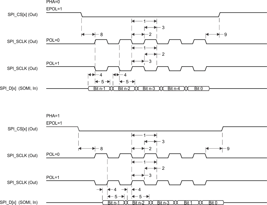 Figure 7-90 SPI Master Mode Receive Timing
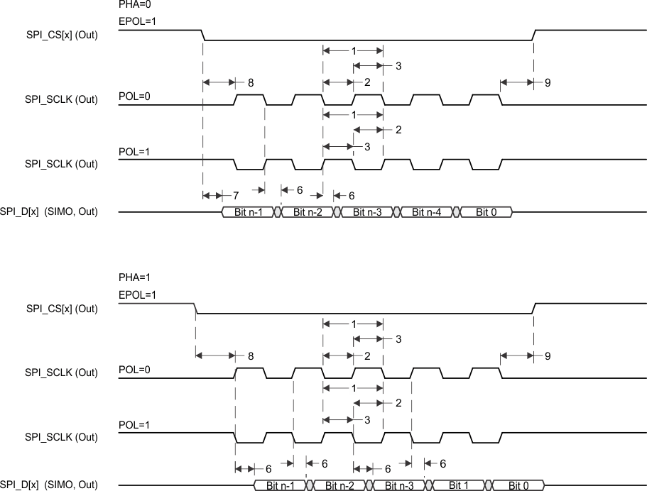 Figure 7-91 SPI Master Mode Transmit Timing
7.13 Multimedia Card (MMC) Interface
For more information, see the Multimedia Card (MMC) section of the AM335x and AMIC110 Sitara Processors Technical Reference Manual.
7.13.1 MMC Electrical Data and Timing
Table 7-86 MMC Timing Conditions
| PARAMETER | MIN | TYP | MAX | UNIT | |
|---|---|---|---|---|---|
| Input Conditions | |||||
| tr | Input signal rise time | 1 | 5 | ns | |
| tf | Input signal fall time | 1 | 5 | ns | |
| Output Condition | |||||
| Cload | Output load capacitance | 3 | 30 | pF | |
Table 7-87 Timing Requirements for MMC[x]_CMD and MMC[x]_DAT[7:0]
(see Figure 7-92)| NO. | 1.8-V MODE | 3.3-V MODE | UNIT | ||||||||
|---|---|---|---|---|---|---|---|---|---|---|---|
| MIN | TYP | MAX | MIN | TYP | MAX | ||||||
| 1 | tsu(CMDV-CLKH) | Setup time, MMC_CMD valid before MMC_CLK rising clock edge | 4.1 | 4.1 | ns | ||||||
| 2 | th(CLKH-CMDV) | Hold time, MMC_CMD valid after MMC_CLK rising clock edge | Industrial extended temperature (–40°C to 125°C) |
MMC0-2 | 3.76 | 3.76 | ns | ||||
| All other temperature ranges | MMC0 | 3.76 | 2.52 | ||||||||
| MMC1 | 3.76 | 3.03 | |||||||||
| MMC2 | 3.76 | 3.0 | |||||||||
| 3 | tsu(DATV-CLKH) | Setup time, MMC_DATx valid before MMC_CLK rising clock edge | 4.1 | 4.1 | ns | ||||||
| 4 | th(CLKH-DATV) | Hold time, MMC_DATx valid after MMC_CLK rising clock edge | Industrial extended temperature (–40°C to 125°C) |
MMC0-2 | 3.76 | 3.76 | ns | ||||
| All other temperature ranges | MMC0 | 3.76 | 2.52 | ||||||||
| MMC1 | 3.76 | 3.03 | |||||||||
| MMC2 | 3.76 | 3.0 | |||||||||
![AM3359 AM3358 AM3357 AM3356 AM3354 AM3352 AM3351 MMC[x]_CMD and
MMC[x]_DAT[7:0] Input Timing AM3359 AM3358 AM3357 AM3356 AM3354 AM3352 AM3351 td_mmc_input_sprs717.gif](/ods/images/JAJSDZ0J/td_mmc_input_sprs717.gif) Figure 7-92 MMC[x]_CMD and MMC[x]_DAT[7:0] Input Timing
Figure 7-92 MMC[x]_CMD and MMC[x]_DAT[7:0] Input Timing
Table 7-88 Switching Characteristics for MMC[x]_CLK
(see Figure 7-93)| NO. | PARAMETER | STANDARD MODE | HIGH-SPEED MODE | UNIT | |||||
|---|---|---|---|---|---|---|---|---|---|
| MIN | TYP | MAX | MIN | TYP | MAX | ||||
| 5 | ƒop(CLK) | Operating frequency, MMC_CLK | 24 | 48 | MHz | ||||
| tcop(CLK) | Operating period: MMC_CLK | 41.7 | 20.8 | ns | |||||
| fid(CLK) | Identification mode frequency, MMC_CLK | 400 | 400 | kHz | |||||
| tcid(CLK) | Identification mode period: MMC_CLK | 2500 | 2500 | ns | |||||
| 6 | tw(CLKL) | Pulse duration, MMC_CLK low | (0.5 × P) – tf(CLK)(1) | (0.5 × P) – tf(CLK)(1) | ns | ||||
| 7 | tw(CLKH) | Pulse duration, MMC_CLK high | (0.5 × P) – tr(CLK)(1) | (0.5 × P) – tr(CLK)(1) | ns | ||||
| 8 | tr(CLK) | Rise time, all signals (10% to 90%) | 2.2 | 2.2 | ns | ||||
| 9 | tf(CLK) | Fall time, all signals (10% to 90%) | 2.2 | 2.2 | ns | ||||
- P = MMC_CLK period
![AM3359 AM3358 AM3357 AM3356 AM3354 AM3352 AM3351 MMC[x]_CLK
Timing AM3359 AM3358 AM3357 AM3356 AM3354 AM3352 AM3351 td_mmc_clk_sprs717.gif](/ods/images/JAJSDZ0J/td_mmc_clk_sprs717.gif) Figure 7-93 MMC[x]_CLK Timing
Figure 7-93 MMC[x]_CLK Timing
Table 7-89 Switching Characteristics for MMC[x]_CMD and MMC[x]_DAT[7:0]—Standard Mode
(see Figure 7-94)| NO. | PARAMETER | OPP100 | OPP50 | UNIT | |||||
|---|---|---|---|---|---|---|---|---|---|
| MIN | TYP | MAX | MIN | TYP | MAX | ||||
| 10 | td(CLKL-CMD) | Delay time, MMC_CLK falling clock edge to MMC_CMD transition | –4 | 14 | –4 | 17.5 | ns | ||
| 11 | td(CLKL-DAT) | Delay time, MMC_CLK falling clock edge to MMC_DATx transition | –4 | 14 | –4 | 17.5 | ns | ||
![AM3359 AM3358 AM3357 AM3356 AM3354 AM3352 AM3351 MMC[x]_CMD and
MMC[x]_DAT[7:0] Output Timing—Standard Mode AM3359 AM3358 AM3357 AM3356 AM3354 AM3352 AM3351 td_mmc_out_std_sprs717.gif](/ods/images/JAJSDZ0J/td_mmc_out_std_sprs717.gif) Figure 7-94 MMC[x]_CMD and MMC[x]_DAT[7:0] Output Timing—Standard Mode
Figure 7-94 MMC[x]_CMD and MMC[x]_DAT[7:0] Output Timing—Standard Mode
Table 7-90 Switching Characteristics for MMC[x]_CMD and MMC[x]_DAT[7:0]—High-Speed Mode
(see Figure 7-95)| NO. | PARAMETER | OPP100 | OPP50 | UNIT | |||||
|---|---|---|---|---|---|---|---|---|---|
| MIN | TYP | MAX | MIN | TYP | MAX | ||||
| 12 | td(CLKL-CMD) | Delay time, MMC_CLK rising clock edge to MMC_CMD transition | 3 | 14 | 3 | 17.5 | ns | ||
| 13 | td(CLKL-DAT) | Delay time, MMC_CLK rising clock edge to MMC_DATx transition | 3 | 14 | 3 | 17.5 | ns | ||
![AM3359 AM3358 AM3357 AM3356 AM3354 AM3352 AM3351 MMC[x]_CMD and
MMC[x]_DAT[7:0] Output Timing—High-Speed Mode AM3359 AM3358 AM3357 AM3356 AM3354 AM3352 AM3351 td_mmc_out_hs_sprs717.gif](/ods/images/JAJSDZ0J/td_mmc_out_hs_sprs717.gif) Figure 7-95 MMC[x]_CMD and MMC[x]_DAT[7:0] Output Timing—High-Speed Mode
Figure 7-95 MMC[x]_CMD and MMC[x]_DAT[7:0] Output Timing—High-Speed Mode
7.14 Programmable Real-Time Unit Subsystem and Industrial Communication Subsystem (PRU-ICSS)
For more information, see the Programmable Real-Time Unit Subsystem and Industrial Communication Subsystem Interface (PRU-ICSS) section of the AM335x and AMIC110 Sitara Processors Technical Reference Manual.
7.14.1 Programmable Real-Time Unit (PRU-ICSS PRU)
Table 7-91 PRU-ICSS PRU Timing Conditions
| PARAMETER | MIN | MAX | UNIT | |
|---|---|---|---|---|
| Output Condition | ||||
| Cload | Capacitive load for each bus line | 30 | pF | |
7.14.1.1 PRU-ICSS PRU Direct Input/Output Mode Electrical Data and Timing
Table 7-92 PRU-ICSS PRU Timing Requirements - Direct Input Mode
(see Figure 7-96)| NO. | MIN | MAX | UNIT | |||
|---|---|---|---|---|---|---|
| 1 | tw(GPI) | Pulse width, GPI | 2 × P(1) | ns | ||
| 2 | tr(GPI) | Rise time, GPI | 1.00 | 3.00 | ns | |
| tf(GPI) | Fall time, GPI | 1.00 | 3.00 | ns | ||
| 3 | tsk(GPI) | Internal skew between GPI[n:0] signals(2) | PRU0 | 1.00 | ns | |
| PRU1 | 3.00 | |||||
 Figure 7-96 PRU-ICSS PRU Direct Input Timing
Table 7-93 PRU-ICSS PRU Switching Requirements – Direct Output Mode
(see Figure 7-69)| NO. | PARAMETER | MIN | MAX | UNIT | ||
|---|---|---|---|---|---|---|
| 1 | tw(GPO) | Pulse width, GPO | 2 × P(1) | ns | ||
| 2 | tr(GPO) | Rise time, GPO | 1.00 | 3.00 | ns | |
| tf(GPO) | Fall time, GPO | 1.00 | 3.00 | ns | ||
| 3 | tsk(GPO) | Internal skew between GPO[n:0] signals(2) | PRU0 | 1.00 | ns | |
| PRU1 | 5.00 | |||||
 Figure 7-97 PRU-ICSS PRU Direct Output Timing
7.14.1.2 PRU-ICSS PRU Parallel Capture Mode Electrical Data and Timing
Table 7-94 PRU-ICSS PRU Timing Requirements - Parallel Capture Mode
(see Figure 7-98 and Figure 7-99)| NO. | MIN | MAX | UNIT | ||
|---|---|---|---|---|---|
| 1 | tc(CLOCKIN) | Cycle time, CLOCKIN | 20.00 | ns | |
| 2 | tw(CLOCKIN_L) | Pulse duration, CLOCKIN low | 10.00 | ns | |
| 3 | tw(CLOCKIN_H) | Pulse duration, CLOCKIN high | 10.00 | ns | |
| 4 | tr(CLOCKIN) | Rising time, CLOCKIN | 1.00 | 3.00 | ns |
| 5 | tf(CLOCKIN) | Falling time, CLOCKIN | 1.00 | 3.00 | ns |
| 6 | tsu(DATAIN-CLOCKIN) | Setup time, DATAIN valid before CLOCKIN | 5.00 | ns | |
| 7 | th(CLOCKIN-DATAIN) | Hold time, DATAIN valid after CLOCKIN | 0.00 | ns | |
| 8 | tr(DATAIN) | Rising time, DATAIN | 1.00 | 3.00 | ns |
| tf(DATAIN) | Falling time, DATAIN | 1.00 | 3.00 | ns | |
 Figure 7-98 PRU-ICSS PRU Parallel Capture Timing - Rising Edge Mode
 Figure 7-99 PRU-ICSS PRU Parallel Capture Timing - Falling Edge Mode
7.14.1.3 PRU-ICSS PRU Shift Mode Electrical Data and Timing
Table 7-95 PRU-ICSS PRU Timing Requirements – Shift In Mode
(see Figure 7-100)| NO. | MIN | MAX | UNIT | ||
|---|---|---|---|---|---|
| 1 | tc(DATAIN) | Cycle time, DATAIN | 10.00 | ns | |
| 2 | tw(DATAIN) | Pulse width, DATAIN | 0.45 × P(1) | 0.55 × P(1) | ns |
| 3 | tr(DATAIN) | Rising time, DATAIN | 1.00 | 3.00 | ns |
| 4 | tf(DATAIN) | Falling time, DATAIN | 1.00 | 3.00 | ns |
 Figure 7-100 PRU-ICSS PRU Shift In Timing
Table 7-96 PRU-ICSS PRU Switching Requirements - Shift Out Mode
(see Figure 7-101)| NO. | MIN | MAX | UNIT | ||
|---|---|---|---|---|---|
| 1 | tc(CLOCKOUT) | Cycle time, CLOCKOUT | 10.00 | ns | |
| 2 | tw(CLOCKOUT) | Pulse width, CLOCKOUT | 0.45 × P(1) | 0.55 × P(1) | ns |
| 3 | tr(CLOCKOUT) | Rising time, CLOCKOUT | 1.00 | 3.00 | ns |
| 4 | tf(CLOCKOUT) | Falling time, CLOCKOUT | 1.00 | 3.00 | ns |
| 5 | td(CLOCKOUT-DATAOUT) | Delay time, CLOCKOUT to DATAOUT valid | 0.00 | 3.00 | ns |
| 6 | tr(DATAOUT) | Rising time, DATAOUT | 1.00 | 3.00 | ns |
| tf(DATAOUT) | Falling time, DATAOUT | 1.00 | 3.00 | ns | |
 Figure 7-101 PRU-ICSS PRU Shift Out Timing
7.14.2 PRU-ICSS EtherCAT (PRU-ICSS ECAT)
Table 7-97 PRU-ICSS ECAT Timing Conditions
| PARAMETER | MIN | MAX | UNIT | |
|---|---|---|---|---|
| Output Condition | ||||
| Cload | Capacitive load for each bus line | 30 | pF | |
7.14.2.1 PRU-ICSS ECAT Electrical Data and Timing
Table 7-98 PRU-ICSS ECAT Timing Requirements – Input Validated With LATCH_IN
(see Figure 7-102)| NO. | MIN | MAX | UNIT | ||
|---|---|---|---|---|---|
| 1 | tw(EDIO_LATCH_IN) | Pulse width, EDIO_LATCH_IN | 100.00 | ns | |
| 2 | tr(EDIO_LATCH_IN) | Rising time, EDIO_LATCH_IN | 1.00 | 3.00 | ns |
| 3 | tf(EDIO_LATCH_IN) | Falling time, EDIO_LATCH_IN | 1.00 | 3.00 | ns |
| 4 | tsu(EDIO_DATA_IN-EDIO_LATCH_IN) | Setup time, EDIO_DATA_IN valid before EDIO_LATCH_IN active edge | 20.00 | ns | |
| 5 | th(EDIO_LATCH_IN-EDIO_DATA_IN) | Hold time, EDIO_DATA_IN valid after EDIO_LATCH_IN active edge | 20.00 | ns | |
| 6 | tr(EDIO_DATA_IN) | Rising time, EDIO_DATA_IN | 1.00 | 3.00 | ns |
| tf(EDIO_DATA_IN) | Falling time, EDIO_DATA_IN | 1.00 | 3.00 | ns | |
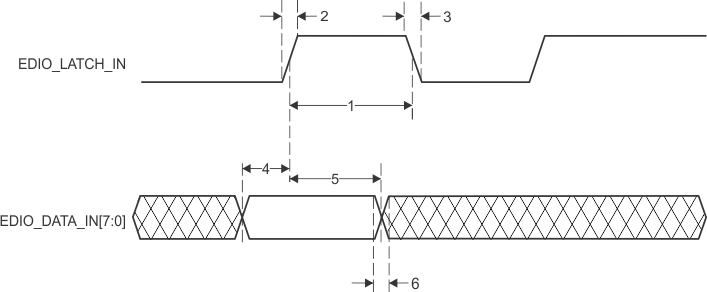 Figure 7-102 PRU-ICSS ECAT Input Validated With LATCH_IN Timing
Table 7-99 PRU-ICSS ECAT Timing Requirements – Input Validated With SYNCx
(see Figure 7-103)| NO. | MIN | MAX | UNIT | ||
|---|---|---|---|---|---|
| 1 | tw(EDC_SYNCx_OUT) | Pulse width, EDC_SYNCx_OUT | 100.00 | ns | |
| 2 | tr(EDC_SYNCx_OUT) | Rising time, EDC_SYNCx_OUT | 1.00 | 3.00 | ns |
| 3 | tf(EDC_SYNCx_OUT) | Falling time, EDC_SYNCx_OUT | 1.00 | 3.00 | ns |
| 4 | tsu(EDIO_DATA_IN-EDC_SYNCx_OUT) | Setup time, EDIO_DATA_IN valid before EDC_SYNCx_OUT active edge | 20.00 | ns | |
| 5 | th(EDC_SYNCx_OUT-EDIO_DATA_IN) | Hold time, EDIO_DATA_IN valid after EDC_SYNCx_OUT active edge | 20.00 | ns | |
| 6 | tr(EDIO_DATA_IN) | Rising time, EDIO_DATA_IN | 1.00 | 3.00 | ns |
| tf(EDIO_DATA_IN) | Falling time, EDIO_DATA_IN | 1.00 | 3.00 | ns | |
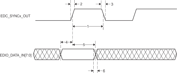 Figure 7-103 PRU-ICSS ECAT Input Validated With SYNCx Timing
Table 7-100 PRU-ICSS ECAT Timing Requirements – Input Validated With Start of Frame (SOF)
(see Figure 7-104)| NO. | MIN | MAX | UNIT | ||
|---|---|---|---|---|---|
| 1 | tw(EDIO_SOF) | Pulse duration, EDIO_SOF | 4 × P(1) | 5 × P(1) | ns |
| 2 | tr(EDIO_SOF) | Rising time, EDIO_SOF | 1.00 | 3.00 | ns |
| 3 | tf(EDIO_SOF) | Falling time, EDIO_SOF | 1.00 | 3.00 | ns |
| 4 | tsu(EDIO_DATA_IN-EDIO_SOF) | Setup time, EDIO_DATA_IN valid before EDIO_SOF active edge | 20.00 | ns | |
| 5 | th(EDIO_SOF-EDIO_DATA_IN) | Hold time, EDIO_DATA_IN valid after EDIO_SOF active edge | 20.00 | ns | |
| 6 | tr(EDIO_DATA_IN) | Rising time, EDIO_DATA_IN | 1.00 | 3.00 | ns |
| tf(EDIO_DATA_IN) | Falling time, EDIO_DATA_IN | 1.00 | 3.00 | ns | |
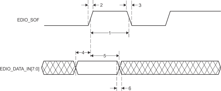 Figure 7-104 PRU-ICSS ECAT Input Validated With SOF
Table 7-101 PRU-ICSS ECAT Timing Requirements - LATCHx_IN
(see Figure 7-105)| NO. | MIN | MAX | UNIT | ||
|---|---|---|---|---|---|
| 1 | tw(EDC_LATCHx_IN) | Pulse duration, EDC_LATCHx_IN | 3 × P(1) | ns | |
| 2 | tr(EDC_LATCHx_IN) | Rising time, EDC_LATCHx_IN | 1.00 | 3.00 | ns |
| 3 | tf(EDC_LATCHx_IN) | Falling time, EDC_LATCHx_IN | 1.00 | 3.00 | ns |
 Figure 7-105 PRU-ICSS ECAT LATCHx_IN Timing
Table 7-102 PRU-ICSS ECAT Switching Requirements - Digital I/Os
| NO. | PARAMETER | MIN | MAX | UNIT | |
|---|---|---|---|---|---|
| 1 | tw(EDIO_OUTVALID) | Pulse duration, EDIO_OUTVALID | 14 × P(1) | 32 × P(1) | ns |
| 2 | tr(EDIO_OUTVALID) | Rising time, EDIO_OUTVALID | 1.00 | 3.00 | ns |
| 3 | tf(EDIO_OUTVALID) | Falling time, EDIO_OUTVALID | 1.00 | 3.00 | ns |
| 4 | td(EDIO_OUTVALID-EDIO_DATA_OUT) | Delay time, EDIO_OUTVALID to EDIO_DATA_OUT | 0.00 | 18 × P(1) | ns |
| 5 | tr(EDIO_DATA_OUT) | Rising time, EDIO_DATA_OUT | 1.00 | 3.00 | ns |
| 6 | tf(EDIO_DATA_OUT) | Falling time, EDIO_DATA_OUT | 1.00 | 3.00 | ns |
| 7 | tsk(EDIO_DATA_OUT) | EDIO_DATA_OUT skew | 8.00 | ns | |
7.14.3 PRU-ICSS MII_RT and Switch
Table 7-103 PRU-ICSS MII_RT Switch Timing Conditions
| PARAMETER | MIN | TYP | MAX | UNIT | |
|---|---|---|---|---|---|
| Input Conditions | |||||
| tR | Input signal rise time | 1(1) | 3(1) | ns | |
| tF | Input signal fall time | 1(1) | 3(1) | ns | |
| Output Condition | |||||
| CLOAD | Output load capacitance | 3 | 20 | pF | |
7.14.3.1 PRU-ICSS MDIO Electrical Data and Timing
Table 7-104 PRU-ICSS MDIO Timing Requirements – MDIO_DATA
(see Figure 7-106)| NO. | MIN | TYP | MAX | UNIT | ||
|---|---|---|---|---|---|---|
| 1 | tsu(MDIO-MDC) | Setup time, MDIO valid before MDC high | 90 | ns | ||
| 2 | th(MDIO-MDC) | Hold time, MDIO valid from MDC high | 0 | ns | ||
 Figure 7-106 PRU-ICSS MDIO_DATA Timing - Input Mode
Table 7-105 PRU-ICSS MDIO Switching Characteristics - MDIO_CLK
(see Figure 7-107)| NO. | PARAMETER | MIN | TYP | MAX | UNIT | |
|---|---|---|---|---|---|---|
| 1 | tc(MDC) | Cycle time, MDC | 400 | ns | ||
| 2 | tw(MDCH) | Pulse duration, MDC high | 160 | ns | ||
| 3 | tw(MDCL) | Pulse duration, MDC low | 160 | ns | ||
| 4 | tt(MDC) | Transition time, MDC | 5 | ns | ||
 Figure 7-107 PRU-ICSS MDIO_CLK Timing
Table 7-106 PRU-ICSS MDIO Switching Characteristics – MDIO_DATA
(see Figure 7-108)| NO. | MIN | TYP | MAX | UNIT | ||
|---|---|---|---|---|---|---|
| 1 | td(MDC-MDIO) | Delay time, MDC high to MDIO valid | 10 | 390 | ns | |
 Figure 7-108 PRU-ICSS MDIO_DATA Timing – Output Mode
7.14.3.2 PRU-ICSS MII_RT Electrical Data and Timing
NOTE
In order to guarantee the MII_RT I/O timing values published in the device data manual, the PRU ocp_clk clock must be configured for 200 MHz (default value) and the TX_CLK_DELAY bit field in the PRUSS_MII_RT_TXCFG0/1 register must be set to 6 h (non-default value).
Table 7-107 PRU-ICSS MII_RT Timing Requirements – MII_RXCLK
(see Figure 7-109)| NO. | 10 Mbps | 100 Mbps | UNIT | ||||||
|---|---|---|---|---|---|---|---|---|---|
| MIN | TYP | MAX | MIN | TYP | MAX | ||||
| 1 | tc(RX_CLK) | Cycle time, RX_CLK | 399.96 | 400.04 | 39.996 | 40.004 | ns | ||
| 2 | tw(RX_CLKH) | Pulse duration, RX_CLK high | 140 | 260 | 14 | 26 | ns | ||
| 3 | tw(RX_CLKL) | Pulse duration, RX_CLK low | 140 | 260 | 14 | 26 | ns | ||
| 4 | tt(RX_CLK) | Transition time, RX_CLK | 3 | 3 | ns | ||||
 Figure 7-109 PRU-ICSS MII_RXCLK Timing
Table 7-108 PRU-ICSS MII_RT Timing Requirements - MII[x]_TXCLK
(see Figure 7-110)| NO. | 10 Mbps | 100 Mbps | UNIT | ||||||
|---|---|---|---|---|---|---|---|---|---|
| MIN | TYP | MAX | MIN | TYP | MAX | ||||
| 1 | tc(TX_CLK) | Cycle time, TX_CLK | 399.96 | 400.04 | 39.996 | 40.004 | ns | ||
| 2 | tw(TX_CLKH) | Pulse duration, TX_CLK high | 140 | 260 | 14 | 26 | ns | ||
| 3 | tw(TX_CLKL) | Pulse duration, TX_CLK low | 140 | 260 | 14 | 26 | ns | ||
| 4 | tt(TX_CLK) | Transition time, TX_CLK | 3 | 3 | ns | ||||
 Figure 7-110 PRU-ICSS MII_TXCLK Timing
Table 7-109 PRU-ICSS MII_RT Timing Requirements - MII_RXD[3:0], MII_RXDV, and MII_RXER
(see Figure 7-111)| NO. | 10 Mbps | 100 Mbps | UNIT | ||||||
|---|---|---|---|---|---|---|---|---|---|
| MIN | TYP | MAX | MIN | TYP | MAX | ||||
| 1 | tsu(RXD-RX_CLK) | Setup time, RXD[3:0] valid before RX_CLK | 8 | 8 | ns | ||||
| tsu(RX_DV-RX_CLK) | Setup time, RX_DV valid before RX_CLK | ||||||||
| tsu(RX_ER-RX_CLK) | Setup time, RX_ER valid before RX_CLK | ||||||||
| 2 | th(RX_CLK-RXD) | Hold time RXD[3:0] valid after RX_CLK | 8 | 8 | ns | ||||
| th(RX_CLK-RX_DV) | Hold time RX_DV valid after RX_CLK | ||||||||
| th(RX_CLK-RX_ER) | Hold time RX_ER valid after RX_CLK | ||||||||
![AM3359 AM3358 AM3357 AM3356 AM3354 AM3352 AM3351 PRU-ICSS MII_RXD[3:0],
MII_RXDV, and MII_RXER Timing AM3359 AM3358 AM3357 AM3356 AM3354 AM3352 AM3351 td_emac_pr_mii_rxd_sprs851.gif](/ods/images/JAJSDZ0J/td_emac_pr_mii_rxd_sprs851.gif) Figure 7-111 PRU-ICSS MII_RXD[3:0], MII_RXDV, and MII_RXER Timing
Figure 7-111 PRU-ICSS MII_RXD[3:0], MII_RXDV, and MII_RXER Timing
Table 7-110 PRU-ICSS MII_RT Switching Characteristics - MII_TXD[3:0] and MII_TXEN
(see Figure 7-112)| NO. | 10 Mbps | 100 Mbps | UNIT | ||||||
|---|---|---|---|---|---|---|---|---|---|
| MIN | TYP | MAX | MIN | TYP | MAX | ||||
| 1 | td(TX_CLK-TXD) | Delay time, TX_CLK high to TXD[3:0] valid | 5 | 25 | 5 | 25 | ns | ||
| td(TX_CLK-TX_EN) | Delay time, TX_CLK to TX_EN valid | ||||||||
![AM3359 AM3358 AM3357 AM3356 AM3354 AM3352 AM3351 PRU-ICSS MII_TXD[3:0],
MII_TXEN Timing AM3359 AM3358 AM3357 AM3356 AM3354 AM3352 AM3351 td_emac_pr_mii_txd_sprs851.gif](/ods/images/JAJSDZ0J/td_emac_pr_mii_txd_sprs851.gif) Figure 7-112 PRU-ICSS MII_TXD[3:0], MII_TXEN Timing
Figure 7-112 PRU-ICSS MII_TXD[3:0], MII_TXEN Timing
7.14.4 PRU-ICSS Universal Asynchronous Receiver Transmitter (PRU-ICSS UART)
Table 7-111 Timing Requirements for PRU-ICSS UART Receive
(see Figure 7-113)| NO. | MIN | MAX | UNIT | ||
|---|---|---|---|---|---|
| 3 | tw(RX) | Pulse duration, receive start, stop, data bit | 0.96U(1) | 1.05U(1) | ns |
Table 7-112 Switching Characteristics Over Recommended Operating Conditions for PRU-ICSS UART Transmit
(see Figure 7-113)| NO. | PARAMETER | MIN | MAX | UNIT | |
|---|---|---|---|---|---|
| 1 | ƒbaud(baud) | Maximum programmable baud rate | 0 | 12 | MHz |
| 2 | tw(TX) | Pulse duration, transmit start, stop, data bit | U – 2(1) | U + 2(1) | ns |
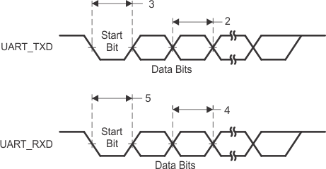 Figure 7-113 PRU-ICSS UART Timing
7.15 Universal Asynchronous Receiver Transmitter (UART)
For more information, see the Universal Asynchronous Receiver Transmitter (UART) section of the AM335x and AMIC110 Sitara Processors Technical Reference Manual.
7.15.1 UART Electrical Data and Timing
Table 7-113 Timing Requirements for UARTx Receive
(see Figure 7-114)| NO. | MIN | MAX | UNIT | ||
|---|---|---|---|---|---|
| 3 | tw(RX) | Pulse duration, receive start, stop, data bit | 0.96U(1) | 1.05U(1) | ns |
- U = UART baud time = 1/programmed baud rate.
Table 7-114 Switching Characteristics for UARTx Transmit
(see Figure 7-114)| NO. | PARAMETER | MIN | MAX | UNIT | |
|---|---|---|---|---|---|
| 1 | ƒbaud(baud) | Maximum programmable baud rate | 3.6864 | MHz | |
| 2 | tw(TX) | Pulse duration, transmit start, stop, data bit | U – 2(1) | U + 2(1) | ns |
- U = UART baud time = 1 / programmed baud rate
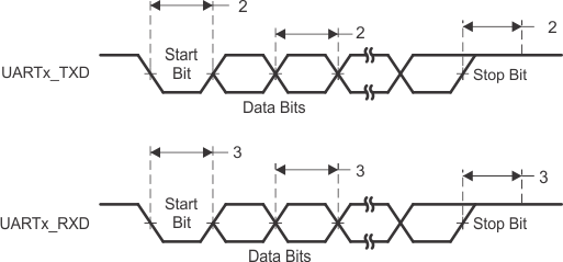 Figure 7-114 UART Timings
7.15.2 UART IrDA Interface
The IrDA module operates in three different modes:
- Slow infrared (SIR) (≤115.2 kbps)
- Medium infrared (MIR) (0.576 Mbps and 1.152 Mbps)
- Fast infrared (FIR) (4 Mbps).
Figure 7-115 shows the UART IrDA pulse parameters. Table 7-115 and Table 7-116 list the signaling rates and pulse durations for UART IrDA receive and transmit modes.
 Figure 7-115 UART IrDA Pulse Parameters
Table 7-115 UART IrDA—Signaling Rate and Pulse Duration—Receive Mode
| SIGNALING RATE | ELECTRICAL PULSE DURATION | UNIT | |
|---|---|---|---|
| MIN | MAX | ||
| SIR | |||
| 2.4 kbps | 1.41 | 88.55 | µs |
| 9.6 kbps | 1.41 | 22.13 | µs |
| 19.2 kbps | 1.41 | 11.07 | µs |
| 38.4 kbps | 1.41 | 5.96 | µs |
| 57.6 kbps | 1.41 | 4.34 | µs |
| 115.2 kbps | 1.41 | 2.23 | µs |
| MIR | |||
| 0.576 Mbps | 297.2 | 518.8 | ns |
| 1.152 Mbps | 149.6 | 258.4 | ns |
| FIR | |||
| 4 Mbps (single pulse) | 67 | 164 | ns |
| 4 Mbps (double pulse) | 190 | 289 | ns |
Table 7-116 UART IrDA—Signaling Rate and Pulse Duration—Transmit Mode
| SIGNALING RATE | ELECTRICAL PULSE DURATION | UNIT | |
|---|---|---|---|
| MIN | MAX | ||
| SIR | |||
| 2.4 kbps | 78.1 | 78.1 | µs |
| 9.6 kbps | 19.5 | 19.5 | µs |
| 19.2 kbps | 9.75 | 9.75 | µs |
| 38.4 kbps | 4.87 | 4.87 | µs |
| 57.6 kbps | 3.25 | 3.25 | µs |
| 115.2 kbps | 1.62 | 1.62 | µs |
| MIR | |||
| 0.576 Mbps | 414 | 419 | ns |
| 1.152 Mbps | 206 | 211 | ns |
| FIR | |||
| 4 Mbps (single pulse) | 123 | 128 | ns |
| 4 Mbps (double pulse) | 248 | 253 | ns |
![AM3359 AM3358 AM3357 AM3356 AM3354 AM3352 AM3351 GMII[x]_RXD[3:0],
GMII[x]_RXDV, GMII[x]_RXER Timing - MII Mode AM3359 AM3358 AM3357 AM3356 AM3354 AM3352 AM3351 td_emac_gmii_rxd_sprs717.gif](/ods/images/JAJSDZ0J/td_emac_gmii_rxd_sprs717.gif)
![AM3359 AM3358 AM3357 AM3356 AM3354 AM3352 AM3351 GMII[x]_TXD[3:0],
GMII[x]_TXEN Timing - MII Mode AM3359 AM3358 AM3357 AM3356 AM3354 AM3352 AM3351 td_emac_gmii_txd_sprs717.gif](/ods/images/JAJSDZ0J/td_emac_gmii_txd_sprs717.gif)
![AM3359 AM3358 AM3357 AM3356 AM3354 AM3352 AM3351 RMII[x]_RXD[1:0],
RMII[x]_CRS_DV, RMII[x]_RXER Timing - RMII Mode AM3359 AM3358 AM3357 AM3356 AM3354 AM3352 AM3351 td_emac_rmii_rxd_sprs717.gif](/ods/images/JAJSDZ0J/td_emac_rmii_rxd_sprs717.gif)
![AM3359 AM3358 AM3357 AM3356 AM3354 AM3352 AM3351 RMII[x]_TXD[1:0],
RMII[x]_TXEN Timing - RMII Mode AM3359 AM3358 AM3357 AM3356 AM3354 AM3352 AM3351 td_emac_rmii_txd_sprs717.gif](/ods/images/JAJSDZ0J/td_emac_rmii_txd_sprs717.gif)
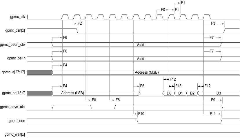
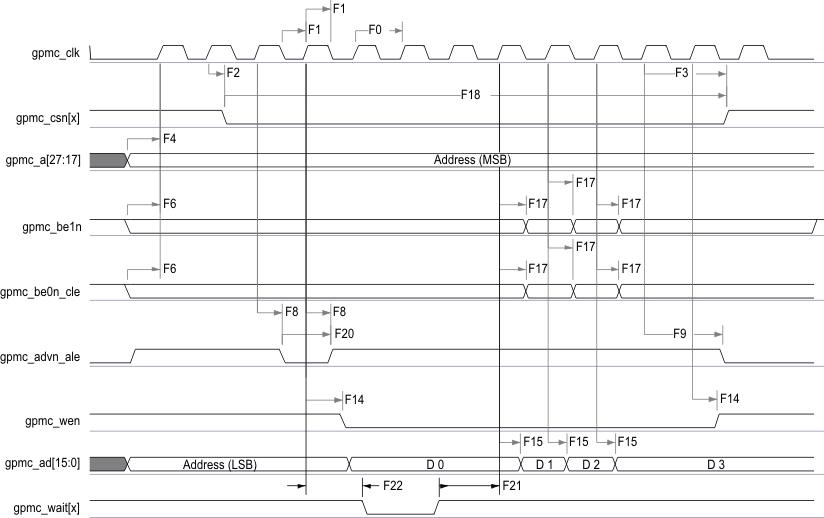
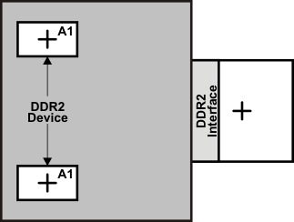
![AM3359 AM3358 AM3357 AM3356 AM3354 AM3352 AM3351 DQS[x] and DQ[x]
Routing and Topology AM3359 AM3358 AM3357 AM3356 AM3354 AM3352 AM3351 ddr2_dqs_dx_rout_topo_sprs717.gif](/ods/images/JAJSDZ0J/ddr2_dqs_dx_rout_topo_sprs717.gif)
