JAJSOY8H November   2011  – July 2022 BQ24160 , BQ24160A , BQ24161 , BQ24161B , BQ24163 , BQ24168

PRODUCTION DATA  

  1. 特長
  2. アプリケーション
  3. 概要
  4. Revision History
  5. Device Comparison Table
  6. Pin Configuration and Functions
  7. Specifications
    1. 7.1 Absolute Maximum Ratings
    2. 7.2 Handling Ratings
    3. 7.3 Recommended Operating Conditions
    4. 7.4 Thermal Information
    5. 7.5 Electrical Characteristics
    6. 7.6 Typical Characteristics
  8. Detailed Description
    1. 8.1 Overview
    2. 8.2 Functional Block Diagram
    3. 8.3 Feature Description
      1. 8.3.1  Charge Mode Operation
        1. 8.3.1.1 Charge Profile
        2. 8.3.1.2 PWM Controller in Charge Mode
      2. 8.3.2  Battery Charging Process
      3. 8.3.3  Battery Detection
      4. 8.3.4  Dynamic Power Path Management (DPPM)
      5. 8.3.5  Input Source Connected
      6. 8.3.6  Battery Only Connected
      7. 8.3.7  Battery Discharge FET (BGATE)
      8. 8.3.8  DEFAULT Mode
      9. 8.3.9  Safety Timer and Watchdog Timer (BQ24160/BQ24161/BQ24161B/BQ24163 only)
      10. 8.3.10 D+, D– Based Adapter Detection for the USB Input (D+, D–, BQ24160/0A/3)
      11. 8.3.11 USB Input Current Limit Selector Input (PSEL, BQ24161/161B/168 only)
      12. 8.3.12 Hardware Chip Disable Input (CD)
      13. 8.3.13 LDO Output (DRV)
      14. 8.3.14 External NTC Monitoring (TS)
      15. 8.3.15 Thermal Regulation and Protection
      16. 8.3.16 Input Voltage Protection in Charge Mode
        1. 8.3.16.1 Sleep Mode
        2. 8.3.16.2 Input Voltage Based DPM
        3. 8.3.16.3 Bad Source Detection
        4. 8.3.16.4 Input Overvoltage Protection
        5. 8.3.16.5 Reverse Boost (Boost Back) Prevention Circuit
      17. 8.3.17 Charge Status Outputs (STAT, INT)
      18. 8.3.18 Good Battery Monitor
    4. 8.4 Device Functional Modes
    5. 8.5 Programming
      1. 8.5.1 Serial Interface Description
        1. 8.5.1.1 F/S Mode Protocol
    6. 8.6 Register Maps
      1. 8.6.1 Status/Control Register (READ/WRITE)
      2. 8.6.2 Battery/ Supply Status Register (READ/WRITE)
      3. 8.6.3 Control Register (READ/WRITE)
      4. 8.6.4 Control/Battery Voltage Register (READ/WRITE)
      5. 8.6.5 Vender/Part/Revision Register (READ only)
      6. 8.6.6 Battery Termination/Fast Charge Current Register (READ/WRITE)
      7. 8.6.7 VIN-DPM Voltage/ DPPM Status Register
      8. 8.6.8 Safety Timer/ NTC Monitor Register (READ/WRITE)
  9. Application and Implementation
    1. 9.1 Application Information
    2. 9.2 Typical Application
      1. 9.2.1 Design Requirements
      2. 9.2.2 Detailed Design Procedure
        1. 9.2.2.1 Output Inductor and Capacitor Selection Guidelines
      3. 9.2.3 Application Curves
  10. 10Power Supply Recommendations
    1. 10.1 Requirements for SYS Output
    2. 10.2 Requirements for Charging
  11. 11Layout
    1. 11.1 Layout Guidelines
    2. 11.2 Layout Example
  12. 12Device and Documentation Support
    1. 12.1 Device Support
      1. 12.1.1 Third-Party Products Disclaimer
    2. 12.2 Receiving Notification of Documentation Updates
    3. 12.3 サポート・リソース
    4. 12.4 Trademarks
    5. 12.5 Electrostatic Discharge Caution
    6. 12.6 Glossary
      1.      Mechanical, Packaging, and Orderable Information

パッケージ・オプション

メカニカル・データ(パッケージ|ピン)
サーマルパッド・メカニカル・データ
発注情報

Typical Characteristics

GUID-612AC087-2622-4B39-952B-CDD59476C52B-low.png
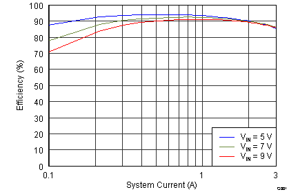
Charge Disabled SYS loaded VBATREG = 3.6 V
IN2500 ILIM
Figure 7-1 IN Efficiency
GUID-B1BE3902-DCE5-4570-9769-09CF0A04C3FE-low.png
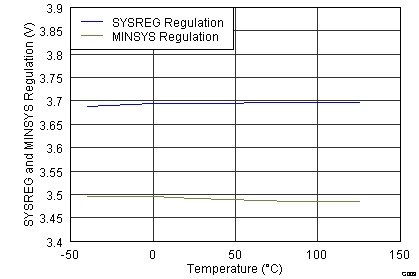
VBAT = 3 V
Figure 7-3 SYSREG and MINSYS Regulation vs Temperature
GUID-0AFD62BB-E10D-46CC-A4AC-531B779BDA69-low.png
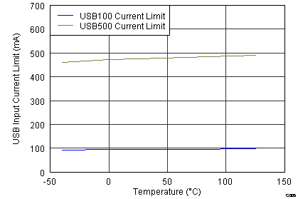
USB100 and USB500 current limit VUSB = 5 V VBAT = 3.6 V
Figure 7-5 USB Input Current Limit vs Temperature
GUID-9A34E8D9-FC86-4616-A632-F48068637694-low.png
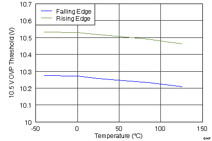
Figure 7-7 10.5-V OVP Threshold vs Temperature
GUID-794AE55A-40CA-4CE1-85DC-CA8E1E44DB5B-low.png
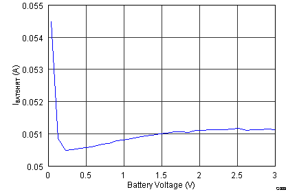
Figure 7-9 IBATSHRT vs Battery Voltage
GUID-C9CD72E8-0485-492B-AF1D-B2917D7931FF-low.png
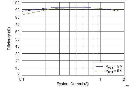
Charge DisabledSYS loadedVBATREG = 3.6 V
USB1500 ILIM
Figure 7-2 USB Efficiency
GUID-93E70C3F-4387-43A2-B7EE-A416789B46F0-low.png
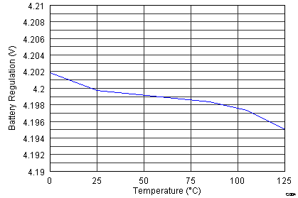
VBATREG = 4.2 V No load Termination Disabled
Figure 7-4 Battery Regulation vs Temperature
GUID-8D516008-29A0-4B02-BC0A-4B56B5E77E4D-low.png
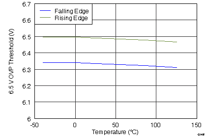
USB input and IN input (BQ24168)
Figure 7-6 6.5-V OVP Threshold vs Temperature
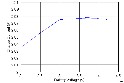
GUID-5D499EE6-4F53-4B89-8085-2F44073A45CE-low.png
ICHARGE = 2 A VIN = 5 V VBATREG = 4.44 V
Figure 7-8 Charge Current vs Battery Voltage