JAJSEG4C December 2013 – July 2018
PRODUCTION DATA.
- 1 特長
- 2 アプリケーション
- 3 概要
- 4 改訂履歴
- 5 Device Comparison Table
- 6 Pin Configuration and Functions
- 7 Specifications
-
8 Detailed Description
- 8.1 Overview
- 8.2 Functional Block Diagram
- 8.3
Feature Description
- 8.3.1 Details of a Qi Wireless Power System and bq51003 Power Transfer Flow Diagrams
- 8.3.2 Dynamic Rectifier Control
- 8.3.3 Dynamic Efficiency Scaling
- 8.3.4 RILIM Calculations
- 8.3.5 Input Overvoltage
- 8.3.6 Adapter Enable Functionality and EN1/EN2 Control
- 8.3.7 End Power Transfer Packet (WPC Header 0x02)
- 8.3.8 Status Outputs
- 8.3.9 WPC Communication Scheme
- 8.3.10 Communication Modulator
- 8.3.11 Adaptive Communication Limit
- 8.3.12 Synchronous Rectification
- 8.3.13 Temperature Sense Resistor Network (TS)
- 8.3.14 3-State Driver Recommendations for the TS-CTRL Pin
- 8.3.15 Thermal Protection
- 8.3.16 WPC v1.2 Compliance – Foreign Object Detection
- 8.4 Device Functional Modes
- 9 Application and Implementation
- 10Power Supply Recommendations
- 11Layout
- 12デバイスおよびドキュメントのサポート
- 13メカニカル、パッケージ、および注文情報
8.3.1 Details of a Qi Wireless Power System and bq51003 Power Transfer Flow Diagrams
The bq51003 integrates a fully compliant WPC v1.2 communication algorithm to streamline receiver designs (no extra software development required). Other unique algorithms such as Dynamic Rectifier Control are also integrated to provide best-in-class system performance. This section provides a high-level overview of these features by illustrating the wireless power transfer flow diagram from start-up to active operation.
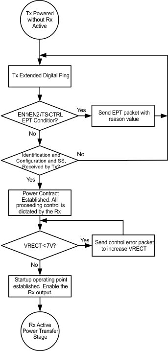
During start-up operation, the wireless power receiver must comply with proper handshaking to be granted a power contract from the Tx. The Tx initiates the hand shake by providing an extended digital ping. If an Rx is present on the Tx surface, the Rx then provides the signal strength, configuration, and identification packets to the Tx (see volume 1 of the WPC specification for details on each packet). These are the first three packets sent to the Tx. The only exception is if there is a true shutdown condition on the EN1/EN2, AD, or TS-CTRL pins where the Rx will shut down the Tx immediately. See Table 5 for details. Once the Tx has successfully received the signal strength, configuration, and identification packets, the Rx will be granted a power contract and is then allowed to control the operating point of the power transfer. With the use of the bq51003 Dynamic Rectifier Control algorithm, the Rx will inform the Tx to adjust the rectifier voltage above 7 V prior to enabling the output supply. This method enhances the transient performance during system start-up. See Figure 18 for the start-up flow diagram details.
 Figure 18. Wireless Power Start-Up Flow Diagram
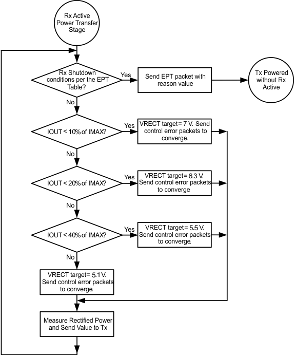
 Once the start-up procedure has been established, the Rx will enter the active power transfer stage. This is considered the main loop of operation. The Dynamic Rectifier Control algorithm will determine the rectifier voltage target based on a percentage of the maximum output current level setting (set by KIMAX and the ILIM resistance to GND). The Rx will send control error packets to converge on these targets. As the output current changes, the rectifier voltage target will dynamically change. As a note, the feedback loop of the WPC system is relatively slow where it can take up to 90 ms to converge on a new rectifier voltage target. It should be understood that the instantaneous transient response of the system is open loop and dependent on the Rx coil output impedance at that operating point. The main loop will also determine if any conditions in Table 5 are true to discontinue power transfer. See Figure 19 which illustrates the active power transfer loop.
 Figure 19. Active Power Transfer Flow Diagram
 Another requirement of the WPC v1.2 specification is to send the measured received power. This task is enabled on the IC by measuring the voltage on the FOD pin which is proportional to the output current and can be scaled based on the choice of the resitor to ground on the FOD pin.