SCAS897A July 2010 – October 2016 CDCLVD1213
PRODUCTION DATA.
- 1 Features
- 2 Applications
- 3 Description
- 4 Revision History
- 5 Pin Configuration and Functions
- 6 Specifications
- 7 Parameter Measurement Information
- 8 Detailed Description
- 9 Application and Implementation
- 10Power Supply Recommendations
- 11Layout
- 12Device and Documentation Support
- 13Mechanical, Packaging, and Orderable Information
パッケージ・オプション
メカニカル・データ(パッケージ|ピン)
- RGT|16
サーマルパッド・メカニカル・データ
- RGT|16
発注情報
1 Features
- 1:4 Differential Buffer
- Low Additive Jitter: < 300-fs RMS in 10-kHz to 20-MHz
- Low Output Skew of 20 ps (Maximum)
- Selectable Divider Ratio 1, /2, /4
- Universal Input Accepts LVDS, LVPECL, and CML
- 4 LVDS Outputs, ANSI EIA/TIA-644A Standard Compatible
- Clock Frequency: Up to 800 MHz
- Device Power Supply: 2.375 V to 2.625 V
- Industrial Temperature Range: –40°C to 85°C
- Packaged in 3 mm × 3 mm, 16-Pin VQFN (RGT)
- ESD Protection Exceeds 3-kV HBM, 1-kV CDM
2 Applications
- Telecommunications and Networking
- Medical Imaging
- Test and Measurement Equipment
- Wireless Communications
- General-Purpose Clocking
3 Description
The CDCLVD1213 clock buffer distributes an input clock to 4 pairs of differential LVDS clock outputs with low additive jitter for clock distribution. The input can either be LVDS, LVPECL, or CML.
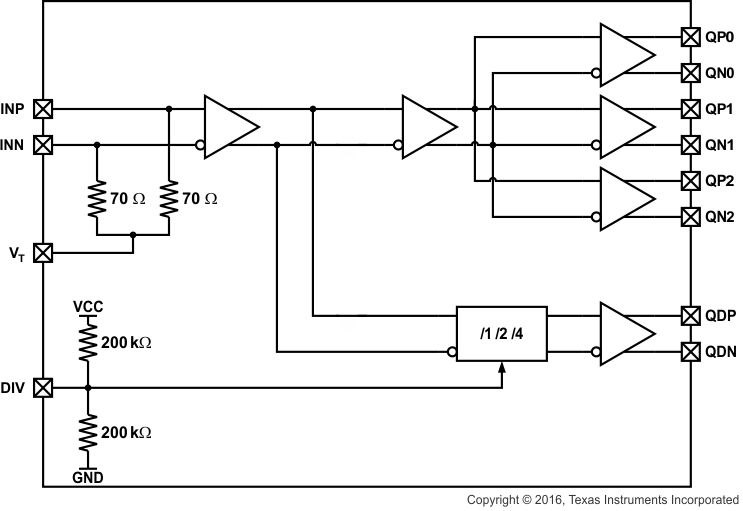
The CDCLVD1213 contains a high performance divider for one output (QD) which can divide the input clock signal by a factor of 1, 2, or 4.
The CDCLVD1213 is specifically designed for driving 50-Ω transmission lines. The part supports a fail-safe function. The device incorporates an input hysteresis which prevents random oscillation of the outputs in the absence of an input signal.
The device operates in 2.5-V supply environment and is characterized from –40°C to 85°C (ambient temperature). The CDCLVD1213 is packaged in small, 16-pin, 3-mm × 3-mm VQFN package.
Device Information(1)
| PART NUMBER | PACKAGE | BODY SIZE (NOM) |
|---|---|---|
| CDCLVD1213 | VQFN (16) | 3.00 mm × 3.00 mm |
- For all available packages, see the orderable addendum at the end of the data sheet.
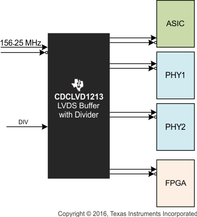
Application Example

CDCLVD1213 Block Diagram
