DLPS119B December 2018 – May 2022 DLP2010NIR
PRODUCTION DATA
- 1 Features
- 2 Applications
- 3 Description
- 4 Revision History
- 5 Pin Configuration and Functions
-
6 Specifications
- 6.1 Absolute Maximum Ratings
- 6.2 Storage Conditions
- 6.3 ESD Ratings
- 6.4 Recommended Operating Conditions
- 6.5 Thermal Information
- 6.6 Electrical Characteristics
- 6.7 Timing Requirements
- 6.8 Switching Characteristics
- 6.9 System Mounting Interface Loads
- 6.10 Physical Characteristics of the Micromirror Array
- 6.11 Micromirror Array Optical Characteristics
- 6.12 Window Characteristics
- 6.13 Chipset Component Usage Specification
- 6.14 Typical Characteristics
- 7 Detailed Description
- 8 Application and Implementation
- 9 Power Supply Recommendations
- 10Layout
- 11Device and Documentation Support
- 12Mechanical, Packaging, and Orderable Information
パッケージ・オプション
デバイスごとのパッケージ図は、PDF版データシートをご参照ください。
メカニカル・データ(パッケージ|ピン)
- FQJ|40
サーマルパッド・メカニカル・データ
発注情報
6.11 Micromirror Array Optical Characteristics
| PARAMETER | TEST CONDITIONS | MIN | NOM | MAX | UNIT | |
|---|---|---|---|---|---|---|
| Micromirror tilt angle | DMD landed state(1) | 17 | degrees | |||
| Micromirror tilt angle tolerance(1) (2) (4) (5) (6) | –1.4 | 1.4 | degrees | |||
| Micromirror tilt direction(3) (7) | Landed ON state | 180 | degrees | |||
| Landed OFF state | 270 | |||||
| Micromirror crossover time | Typical Performance | 1.5 | 4 | μs | ||
| Micromirror switching time | Typical Performance | 6 | ||||
| Image performance(8) | Bright pixel(s) in active area (9) | Gray 10 Screen (10) | 0 | micromirrors | ||
| Bright pixel(s) in the POM (11) | Gray 10 Screen (10) | 1 | ||||
| Dark pixel(s) in the active area (12) | White Screen | 4 | ||||
| Adjacent pixel(s) (13) | Any Screen | 0 | ||||
| Unstable pixel(s) in active area (14) | Any Screen | 0 | ||||
(1) Measured relative to the plane formed by the overall micromirror array.
(2) Additional variation exists between the micromirror array and the package datums.
(3) When the micromirror array is landed (not parked), the tilt direction of each individual micromirror is dictated by the binary contents of the CMOS memory cell associated with each individual micromirror. A binary value
of 1 results in a micromirror landing in the ON State direction. A binary value of 0 results in a micromirror landing in the OFF State direction.
(4) Represents the landed tilt angle variation relative to the nominal landed tilt angle.
(5) Represents the variation that can occur between any two individual micromirrors, located on the same device or located on different devices.
(6) For some applications, it is critical to account for the micromirror tilt angle variation in the overall system optical design. With some system optical designs, the micromirror tilt angle variation within a device may
result in perceivable non-uniformities in the light field reflected from the micromirror array. With some system optical designs, the micromirror tilt angle variation between devices may result in colorimetry variations, system
efficiency variations or system contrast variations.
(7) Micromirror tilt direction is measured as in a typical polar coordinate system: measuring counter-clockwise from a 0° reference which is aligned with the +X Cartesian axis.
(8) Conditions of Acceptance: All DMD image quality returns will be evaluated using
the following projected image test conditions:
Test set degamma shall be linear
Test set brightness and contrast shall be set to nominal
The diagonal size of the projected image shall be a minimum of 20 inches
The projections screen shall be 1X gain
The projected image shall be inspected from a 38 inch minimum viewing distance
The image shall be in focus during all image quality tests
(9) Bright pixel definition: A single pixel or mirror that is stuck in the ON
position and is visibly brighter than the surrounding pixels
(10) Gray 10 screen definition: All areas of the screen are colored with the
following settings:
Red = 10/255
Green = 10/255
Blue = 10/255
Red = 10/255
Green = 10/255
Blue = 10/255
(11) POM definition: Rectangular border of off-state mirrors surrounding the active
area
(12) Dark pixel definition: A single pixel or mirror that is stuck in the OFF
position and is visibly darker than the surrounding pixels
(13) Adjacent pixel definition: Two or more stuck pixels sharing a common border or
common point, also referred to as a cluster
(14) Unstable pixel definition: A single pixel or mirror that does not operate in
sequence with parameters loaded into memory. The unstable pixel appears to be
flickering asynchronously with the image
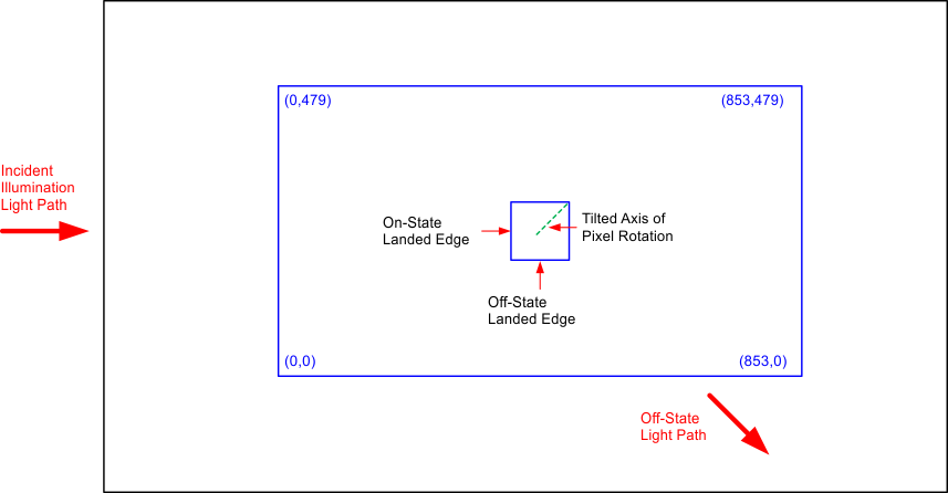
Figure 6-17 Landed Pixel Orientation and Tilt