JAJSGI1B November 2018 – May 2022 DLP4710
PRODUCTION DATA
- 1 特長
- 2 アプリケーション
- 3 概要
- 4 Revision History
- 5 Pin Configuration and Functions
-
6 Specifications
- 6.1 Absolute Maximum Ratings
- 6.2 Storage Conditions
- 6.3 ESD Ratings
- 6.4 Recommended Operating Conditions
- 6.5 Thermal Information
- 6.6 Electrical Characteristics
- 6.7 Timing Requirements
- 6.8 Switching Characteristics
- 6.9 System Mounting Interface Loads
- 6.10 Physical Characteristics of the Micromirror Array
- 6.11 Micromirror Array Optical Characteristics
- 6.12 Window Characteristics
- 6.13 Chipset Component Usage Specification
- 6.14 Software Requirements
- 7 Detailed Description
- 8 Application and Implementation
- 9 Power Supply Recommendations
- 10Layout
- 11Device and Documentation Support
- 12Mechanical, Packaging, and Orderable Information
7.6 Micromirror Array Temperature Calculation
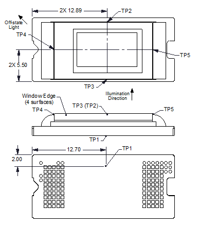
 Figure 7-1 DMD Thermal Test Points
Micromirror array temperature can be computed analytically from measurement points on the outside of the package, the ceramic package thermal resistance, the electrical power dissipation, and the illumination heat load. The relationship between micromirror array temperature and the reference ceramic temperature is provided by the following equations:
where
- TARRAY = Computed DMD array temperature (°C)
- TCERAMIC = Measured ceramic temperature (°C), TP1 location in Figure 7-1
- RARRAY–TO–CERAMIC = DMD package thermal resistance from array to outside ceramic (°C/W) specified in Section 6.5
- QARRAY = Total DMD power; electrical plus absorbed (calculated) (W)
- QELECTRICAL = Nominal DMD electrical power dissipation (W)
- CL2W = Conversion constant for screen lumens to absorbed optical power on the DMD (W/lm) specified below
- SL = Measured ANSI screen lumens (lm)
The electrical power dissipation of the DMD varies and depends on the voltages, data rates and operating frequencies. Use a nominal electrical power dissipation of 0.25 W to calculate array temperature. Absorbed optical power from the illumination source varies and depends on the operating state of the micromirrors and the intensity of the light source. Equations shown above are valid for a 1-chip DMD system with total projection efficiency through the projection lens from DMD to the screen of 87%.
The conversion constant CL2W is based on the DMD micromirror array characteristics. The conversion constant assumes a spectral efficiency of 300 lm/W for the projected light and illumination distribution of 83.7% on the DMD active array, and 16.3% on the DMD array border and window aperture. The conversion constant is calculated to be 0.00266 W/lm.
The following is a sample calculation for typical projection application:
| TCERAMIC = 55°C (measured) | |
| SL = 1500 lm (measured) | |
| QELECTRICAL = 0.25 W | |
| CL2W = 0.00266 W/lm | |
| QARRAY = 0.25 W + (0.00266 W/lm × 1500 lm) = 4.24 W | |
| TARRAY = 55°C + (4.24 W × 1.1°C/W) = 59.66°C |