JAJSHH9H May   2008  – May 2019 DS90LV028AQ-Q1

UNLESS OTHERWISE NOTED, this document contains PRODUCTION DATA.  

  1. 特長
  2. アプリケーション
  3. 概要
    1.     Device Images
      1.      機能図
  4. 改訂履歴
  5. Pin Configuration and Functions
    1.     Pin Descriptions
  6. Specifications
    1. 6.1 Absolute Maximum Ratings
    2. 6.2 ESD Ratings
    3. 6.3 Recommended Operating Conditions
    4. 6.4 Thermal Information
    5. 6.5 Electrical Characteristics
    6. 6.6 Switching Characteristics
    7. 6.7 Typical Performance Curves
  7. Parameter Measurement Information
  8. Detailed Description
    1. 8.1 Functional Block Diagram
    2. 8.2 Device Functional Modes
  9. Application and Implementation
    1. 9.1 Application Information
    2. 9.2 Typical Application
      1. 9.2.1 Detailed Design Procedure
        1. 9.2.1.1 Power Decoupling Recommendations
        2. 9.2.1.2 Termination
        3. 9.2.1.3 Input Failsafe Biasing
        4. 9.2.1.4 Probing LVDS Transmission Lines
        5. 9.2.1.5 Cables and Connectors, General Comments
  10. 10Layout
    1. 10.1 Layout Guidelines
      1. 10.1.1 Differential Traces
      2. 10.1.2 PC Board Considerations
  11. 11デバイスおよびドキュメントのサポート
    1. 11.1 デバイス・サポート
    2. 11.2 コミュニティ・リソース
    3. 11.3 商標
    4. 11.4 静電気放電に関する注意事項
    5. 11.5 Glossary
  12. 12メカニカル、パッケージ、および注文情報

パッケージ・オプション

メカニカル・データ(パッケージ|ピン)
サーマルパッド・メカニカル・データ
発注情報

Pin Configuration and Functions

D Package
SOIC 8 Pin
Top View
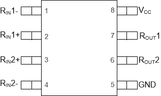
DS90LV028AQ-Q1 D_pinout_SNLS299.gif
DQF Package
WSON 8 Pin
Top View
DS90LV028AQ-Q1 DQF_pinout_SNLS299.gif
DQF - Product Preview

Pin Descriptions

Pin Number Name Description
1 RIN1- Inverting receiver input pin
4 RIN2-
2 RIN1+ Non-inverting receiver input pin
3 RIN2+
6 ROUT2 Receiver output pin
7 ROUT1
8 VCC Power supply pin, +3.3V +/- 0.3V
5 GND Ground pin