JAJSM26C September 2000 – January 2022 INA126 , INA2126
PRODUCTION DATA
- 1 特長
- 2 アプリケーション
- 3 概要
- 4 Revision History
- 5 Pin Configuration and Functions
- 6 Specifications
- 7 Detailed Description
- 8 Application and Implementation
- 9 Power Supply Recommendations
- 10Layout
- 11Device and Documentation Support
- 12Mechanical, Packaging, and Orderable Information
パッケージ・オプション
メカニカル・データ(パッケージ|ピン)
サーマルパッド・メカニカル・データ
- D|8
発注情報
5 Pin Configuration and Functions
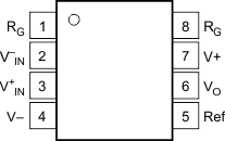
 Figure 5-1 INA126: P (8-Pin PDIP), D
(8-Pin SOIC), and DGK (8-Pin VSSOP) Packages, Top View
Figure 5-1 INA126: P (8-Pin PDIP), D
(8-Pin SOIC), and DGK (8-Pin VSSOP) Packages, Top ViewTable 5-1 Pin Functions: INA126
| PIN | I/O | DESCRIPTION | |
|---|---|---|---|
| NO. | NAME | ||
| 1, 8 | RG | — | Gain setting pin. For gains greater than 5 place a gain resistor between pin 1 and pin 8. |
| 2 | V–IN | I | Negative input |
| 3 | V+IN | I | Positive input |
| 4 | V– | — | Negative supply |
| 5 | Ref | I | Reference input. This pin must be driven by a low impedance or connected to ground. |
| 6 | VO | O | Output |
| 7 | V+ | — | Positive supply |
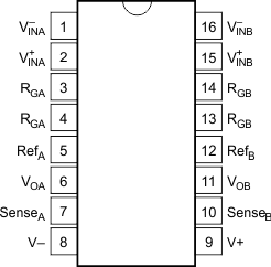
 Figure 5-2 INA2126: N (16-Pin PDIP), D
(16-Pin SOIC), and DBQ (16-Pin SSOP) Packages, Top View
Figure 5-2 INA2126: N (16-Pin PDIP), D
(16-Pin SOIC), and DBQ (16-Pin SSOP) Packages, Top ViewTable 5-2 Pin Functions: INA2126
| PIN | I/O | DESCRIPTION | |
|---|---|---|---|
| NO. | NAME | ||
| 1 | V–INA | I | Negative input for amplifier A |
| 2 | V+INA | I | Positive input for amplifier A |
| 3, 4 | RGA | — | Gain setting pin for amplifier A. For gains greater than 5 place a gain resistor between pin 3 and pin 4. |
| 5 | RefA | I | Reference input for amplifier A. This pin must be driven by a low impedance or connected to ground. |
| 6 | VOA | O | Output of amplifier A |
| 7 | SenseA | I | Feedback for amplifier A. Connect to VOA, amplifier A output. |
| 8 | V– | — | Negative supply |
| 9 | V+ | — | Positive supply |
| 10 | SenseB | I | Feedback for amplifier B. Connect to VOB, amplifier B output. |
| 11 | VOB | O | Output of amplifier B |
| 12 | RefB | I | Reference input for amplifier B. This pin must be driven by a low impedance or connected to ground. |
| 13, 14 | RGB | — | Gain setting pin for amplifier B. For gains greater than 5 place a gain resistor between pin 13 and pin 14. |
| 15 | V+INB | I | Positive input for amplifier B |
| 16 | V–INB | I | Negative input for amplifier B |