JAJSJL2B December 2021 – December 2021 LDC3114-Q1
PRODUCTION DATA
- 1 特長
- 2 アプリケーション
- 3 概要
- 4 Revision History
- 5 Pin Configuration and Functions
- 6 Specifications
-
7 Detailed Description
- 7.1 Overview
- 7.2 Functional Block Diagram
- 7.3 Feature Description
- 7.4 Device Functional Modes
- 7.5 Register Maps
-
8 Application and Implementation
- 8.1
Application Information
- 8.1.1 Theory of Operation
- 8.1.2 Designing Sensor Parameters
- 8.1.3 Setting COM Pin Capacitor
- 8.1.4 Defining Power-On Timing
- 8.1.5 Configuring Button or Raw Data Scan Rate
- 8.1.6 Programming Button or Raw Data Sampling Window
- 8.1.7 Scaling Frequency Counter Output
- 8.1.8 Setting Button Triggering Threshold
- 8.1.9 Tracking Baseline
- 8.1.10 Mitigating False Button Detections
- 8.1.11 Reporting Interrupts for Button Presses, Raw Data Ready and Error Conditions
- 8.1.12 Estimating Supply Current
- 8.2 Typical Application
- 8.1
Application Information
- 9 Power Supply Recommendations
- 10Layout
- 11Device and Documentation Support
- 12Mechanical, Packaging, and Orderable Information
7.3.3 Raw Data Output
Raw data mode is enabled by setting BTN_ALG_EN=0x0 field in Register INTPOL Address 0x11. Figure 7-2 shows that this operation will extract data directly from the output of the inductance-to-digital converter.
The data is read from the I2C interface of the LDC3114-Q1. The DATA_RDY field in Register OUT (Address 0x01) indicates when new data is available for reading. In the raw data mode, the INTB pin also assserted when new data is available and can be used by the MCU as an interrupt. The raw data can be extracted by reading, the output RAW_DATAn_x registers (n = 0, 1, 2, or 3, for each channel, x= 1, 2, or 3 splitting 24-bit data over 3 8-bit register fields). Equation 1 shows the relationship between 24-bit data and the sensor frequency.
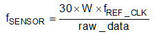
where:
- fsensor is the instantaneous frequency of the inductive sensor
- fREF_CLK is the internal reference clock frequency as specified in Section 6.5
- raw_data is the decimal representation of 24-bit binary data read from the RAW_DATAn_x for a particular channel
- W calculated in Equation 2 (see
Section 8.1.6 for details):Equation 2.