JAJSJL2B December 2021 – December 2021 LDC3114-Q1
PRODUCTION DATA
- 1 特長
- 2 アプリケーション
- 3 概要
- 4 Revision History
- 5 Pin Configuration and Functions
- 6 Specifications
-
7 Detailed Description
- 7.1 Overview
- 7.2 Functional Block Diagram
- 7.3 Feature Description
- 7.4 Device Functional Modes
- 7.5 Register Maps
-
8 Application and Implementation
- 8.1
Application Information
- 8.1.1 Theory of Operation
- 8.1.2 Designing Sensor Parameters
- 8.1.3 Setting COM Pin Capacitor
- 8.1.4 Defining Power-On Timing
- 8.1.5 Configuring Button or Raw Data Scan Rate
- 8.1.6 Programming Button or Raw Data Sampling Window
- 8.1.7 Scaling Frequency Counter Output
- 8.1.8 Setting Button Triggering Threshold
- 8.1.9 Tracking Baseline
- 8.1.10 Mitigating False Button Detections
- 8.1.11 Reporting Interrupts for Button Presses, Raw Data Ready and Error Conditions
- 8.1.12 Estimating Supply Current
- 8.2 Typical Application
- 8.1
Application Information
- 9 Power Supply Recommendations
- 10Layout
- 11Device and Documentation Support
- 12Mechanical, Packaging, and Orderable Information
6.9 Typical Characteristics
Over recommended operating conditions unless specified otherwise. VDD = 1.8 V, TJ = 25°C.One channel enabled with a button sampling window of 1 ms unless specified otherwise.
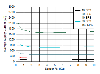 Figure 6-2 Supply Current vs Sensor RP for Normal Power Mode. Sensor
Frequency = 10 MHz. Sampling Window = 2mS. Four Channels Enabled.
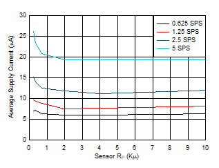 Figure 6-4 Supply Current vs Sensor RP for Low Power Mode. Sensor Frequency
= 10 MHz.
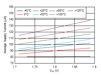 Figure 6-6 Supply Current vs. VDD. Sensor RP = 720 Ω, Scan Rate
= 40 SPS, Sensor Frequency = 20 MHz.
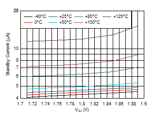 Figure 6-8 Standby Current vs VDD
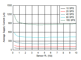 Figure 6-3 Supply Current vs Sensor RP for Normal Power Mode. Sensor
Frequency = 10 MHz. Sampling Window = 2mS. Two Channels Enabled.
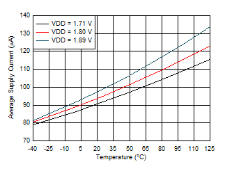 Figure 6-5 Supply Current vs Temperature. Sensor RP = 720 Ω, Scan Rate = 40
SPS, Sensor Frequency = 20 MHz.
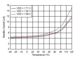 Figure 6-7 Standby Current vs. Temperature
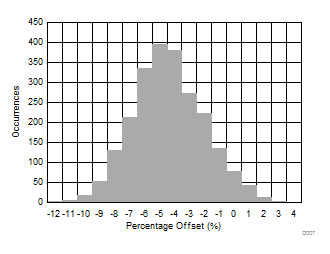 Figure 6-9 Scan Rate Distribution at 30°C