JAJSJX3 December   2021 LDC3114

PRODUCTION DATA  

  1. 特長
  2. アプリケーション
  3. 概要
  4. Revision History
  5. Pin Configuration and Functions
  6. Specifications
    1. 6.1 Absolute Maximum Ratings
    2. 6.2 ESD Ratings
    3. 6.3 Recommended Operating Conditions
    4. 6.4 Thermal Information
    5. 6.5 Electrical Characteristics
    6. 6.6 Digital Interface
    7. 6.7 I2C Interface
    8. 6.8 Timing Diagram
    9. 6.9 Typical Characteristics
  7. Detailed Description
    1. 7.1 Overview
    2. 7.2 Functional Block Diagram
    3. 7.3 Feature Description
      1. 7.3.1 Multimode Operation
      2. 7.3.2 Multichannel and Single-Channel Operation
      3. 7.3.3 Raw Data Output
      4. 7.3.4 Button Output Interfaces
      5. 7.3.5 Programmable Button Sensitivity
      6. 7.3.6 Baseline Tracking
      7. 7.3.7 Integrated Button Algorithms
      8. 7.3.8 I2C Interface
        1. 7.3.8.1 I2C Interface Specifications
        2. 7.3.8.2 I2C Bus Control
    4. 7.4 Device Functional Modes
      1. 7.4.1 Normal Power Mode
      2. 7.4.2 Low Power Mode
      3. 7.4.3 Configuration Mode
    5. 7.5 Register Maps
      1. 7.5.1 LDC3114 Registers
      2. 7.5.2 Gain Table for Registers GAIN0, GAIN1, GAIN2, and GAIN3
  8. Application and Implementation
    1. 8.1 Application Information
      1. 8.1.1  Theory of Operation
      2. 8.1.2  Designing Sensor Parameters
      3. 8.1.3  Setting COM Pin Capacitor
      4. 8.1.4  Defining Power-On Timing
      5. 8.1.5  Configuring Button or Raw Data Scan Rate
      6. 8.1.6  Programming Button or Raw Data Sampling Window
      7. 8.1.7  Scaling Frequency Counter Output
      8. 8.1.8  Setting Button Triggering Threshold
      9. 8.1.9  Tracking Baseline
      10. 8.1.10 Mitigating False Button Detections
        1. 8.1.10.1 Eliminating Common-Mode Change (Anti-Common)
        2. 8.1.10.2 Resolving Simultaneous Button Presses (Max-Win)
        3. 8.1.10.3 Overcoming Case Twisting (Anti-Twist)
        4. 8.1.10.4 Mitigating Metal Deformation (Anti-Deform)
      11. 8.1.11 Reporting Interrupts for Button Presses, Raw Data Ready and Error Conditions
      12. 8.1.12 Estimating Supply Current
    2. 8.2 Typical Application
      1. 8.2.1 Touch Button Design
        1. 8.2.1.1 Design Requirements
        2. 8.2.1.2 Detailed Design Procedure
        3. 8.2.1.3 Application Curves
  9. Power Supply Recommendations
  10. 10Layout
    1. 10.1 Layout Guidelines
    2. 10.2 Layout Example
  11. 11Device and Documentation Support
    1. 11.1 Documentation Support
      1. 11.1.1 Related Documentation
    2. 11.2 Receiving Notification of Documentation Updates
    3. 11.3 サポート・リソース
    4. 11.4 Trademarks
    5. 11.5 Electrostatic Discharge Caution
    6. 11.6 Glossary
  12. 12Mechanical, Packaging, and Orderable Information

パッケージ・オプション

メカニカル・データ(パッケージ|ピン)
サーマルパッド・メカニカル・データ
発注情報

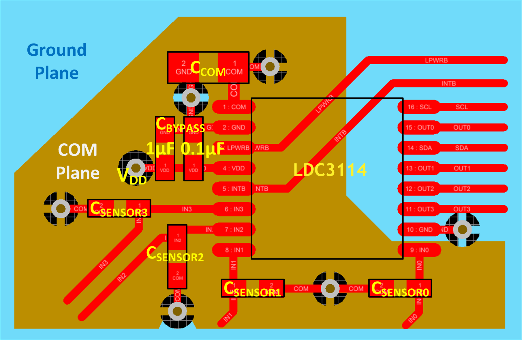
Layout Example

GUID-20210503-CA0I-NHDZ-8RGH-6WGX0K2G2G7Q-low.png Figure 10-1 Layout of LDC3114 (TSSOP-16) With Decoupling Capacitors and Sensor Capacitors