SLCS144E July 2004 – October 2014 LM317L
PRODUCTION DATA.
- 1 Features
- 2 Applications
- 3 Description
- 4 Simplified Schematic
- 5 Revision History
- 6 Pin Configuration and Functions
- 7 Specifications
- 8 Detailed Description
-
9 Application and Implementation
- 9.1 Application Information
- 9.2 Typical Application
- 9.3
General Configurations
- 9.3.1 Regulator Circuit With Improved Ripple Rejection
- 9.3.2 0-V to 30-V Regulator Circuit
- 9.3.3 Precision Current-Limiter Circuit
- 9.3.4 Tracking Preregulator Circuit
- 9.3.5 Slow-Turn On 15-V Regulator Circuit
- 9.3.6 50-mA Constant-Current Battery-Charger Circuit
- 9.3.7 Current-Limited 6-V Charger
- 9.3.8 High-Current Adjustable Regulator
- 10Power Supply Recommendations
- 11Layout
- 12Device and Documentation Support
- 13Mechanical, Packaging, and Orderable Information
パッケージ・オプション
デバイスごとのパッケージ図は、PDF版データシートをご参照ください。
メカニカル・データ(パッケージ|ピン)
- D|8
- PW|8
- PK|3
- LP|3
サーマルパッド・メカニカル・データ
- PK|3
発注情報
9 Application and Implementation
NOTE
Information in the following applications sections is not part of the TI component specification, and TI does not warrant its accuracy or completeness. TI’s customers are responsible for determining suitability of components for their purposes. Customers should validate and test their design implementation to confirm system functionality.
9.1 Application Information
The two output resistors are the only components required to adjust VOUT.
9.2 Typical Application
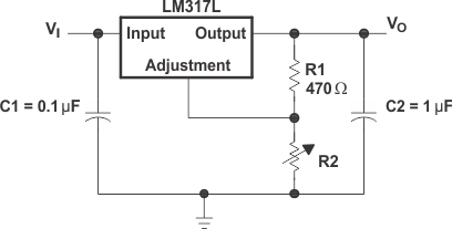
9.2.1 Design Requirements
- Use of an input bypass capacitor is recommended if regulator is far from the filter capacitors.
- For this design example, use the parameters listed in Table 1.
- Use of an output capacitor improves transient response, but is optional.
Table 1. Design Parameters
| DESIGN PARAMETER | EXAMPLE VALUE |
|---|---|
| Input voltage range | (Output Voltage + 2.5 V) to 32 V |
| Output voltage | VREF × (1 + R2 / R1) + IADJ × R2 |
9.2.2 Detailed Design Procedure
9.2.2.1 Input Capacitor
An input capacitor is not required, but it is recommended, particularly if the regulator is not in close proximity to the power-supply filter capacitors. A 0.1-µF ceramic or 1-µF tantalum provides sufficient bypassing for most applications, especially when adjustment and output capacitors are used.
9.2.2.2 Output Capacitor
An output capacitor improves transient response, but it not needed for stability.
9.2.2.3 Feedback Resistors
The feedback resistor set the output voltage using Equation 2.
9.2.2.4 Adjustment Terminal Capacitor
The optional adjustment pin capacitor will improve ripple rejection by preventing the amplification of the ripple. When capacitor is used and VOUT > 6 V, a protection diode from adjust to output is recommended.
9.2.2.5 Design Options and Parameters
Common Linear Regulator designs are concerned with the following parameters:
- Input voltage range
- Input capacitor range
- Output voltage
- Output current rating
- Output capacitor range
- Input short protection
- Stability
- Ripple rejection
9.2.2.6 Output Voltage
VO is calculated as shown in Equation 3.
Because IADJ typically is 50 µA, it is negligible in most applications.
9.2.2.7 Ripple Rejection
CADJ is used to improve ripple rejection; it prevents amplification of the ripple as the output voltage is adjusted higher. If CADJ is used, it is best to include protection diodes.
9.2.2.8 Input Short Protection
If the input is shorted to ground during a fault condition, protection diodes provide measures to prevent the possibility of external capacitors discharging through low-impedance paths in the IC. By providing low-impedance discharge paths for CO and CADJ, respectively, D1 and D2 prevent the capacitors from discharging into the output of the regulator.
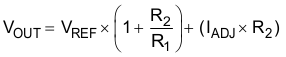
9.2.3 Application Curves
 Figure 2. Adjustment Voltage Relative to Output Over Temperature
9.3 General Configurations
9.3.1 Regulator Circuit With Improved Ripple Rejection
C2 helps to stabilize the voltage at the adjustment pin, which will help reject noise. Diode D1 exists to discharge C2 in case the output is shorted to ground.
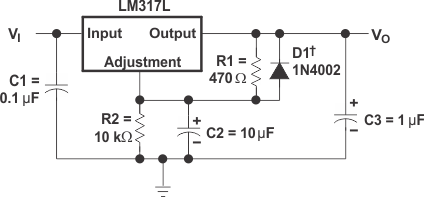 Figure 3. Regulator Circuit With Improved Ripple Rejection
9.3.2 0-V to 30-V Regulator Circuit
In the 0-V to 30-V regulator circuit application, the output voltage is determined by Equation 4.
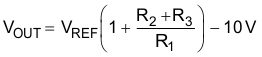
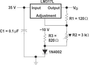 Figure 4. 0-V to 30-V Regulator Circuit
9.3.3 Precision Current-Limiter Circuit
This application will limit the output current to the ILIMIT shown in Figure 5.
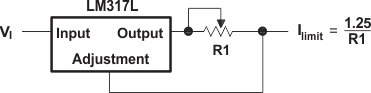 Figure 5. Precision Current-Limiter Circuit
9.3.4 Tracking Preregulator Circuit
The tracking preregulator circuit application keeps a constant voltage across the second LM317L in the circuit.
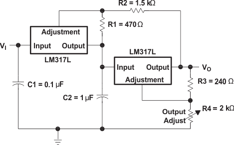 Figure 6. Tracking Preregulator Circuit
9.3.5 Slow-Turn On 15-V Regulator Circuit
The capacitor C1, in combination with the PNP transistor, helps the circuit to slowly start supplying voltage. In the beginning, the capacitor is not charged. Therefore, output voltage will start at 1.9 V, as determined by Equation 5. As the capacitor voltage rises, VOUT will rise at the same rate. When the output voltage reaches the value determined by R1 and R2, the PNP will be turned off.
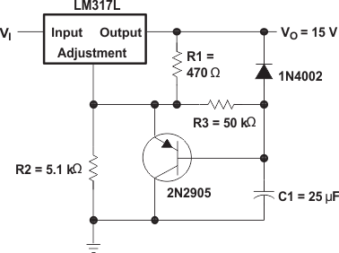 Figure 7. Slow-Turn On 15-V Regulator Circuit
9.3.6 50-mA Constant-Current Battery-Charger Circuit
The current-limit operation mode can be used to trickle charge a battery at a fixed current as determined by Equation 6. VI should be greater than VBAT + 3.75 V.
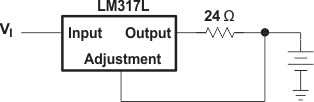 Figure 8. 50-mA Constant-Current Battery-Charger Circuit
9.3.7 Current-Limited 6-V Charger
As the charge current increases, the voltage at the bottom resistor increases until the NPN starts sinking current from the adjustment pin. The voltage at the adjustment pin will drop, and consequently the output voltage will decrease until the NPN stops conducting.
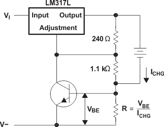 Figure 9. Current-Limited 6-V Charger
9.3.8 High-Current Adjustable Regulator
This application allows higher currents at VOUT than the LM317L device can provide, while still keeping the output voltage at levels determined by the adjustment-pin resistor divider of the LM317L.
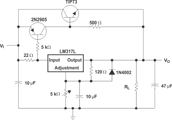 Figure 10. High-Current Adjustable Regulator