SLCS144E July 2004 – October 2014 LM317L
PRODUCTION DATA.
- 1 Features
- 2 Applications
- 3 Description
- 4 Simplified Schematic
- 5 Revision History
- 6 Pin Configuration and Functions
- 7 Specifications
- 8 Detailed Description
-
9 Application and Implementation
- 9.1 Application Information
- 9.2 Typical Application
- 9.3
General Configurations
- 9.3.1 Regulator Circuit With Improved Ripple Rejection
- 9.3.2 0-V to 30-V Regulator Circuit
- 9.3.3 Precision Current-Limiter Circuit
- 9.3.4 Tracking Preregulator Circuit
- 9.3.5 Slow-Turn On 15-V Regulator Circuit
- 9.3.6 50-mA Constant-Current Battery-Charger Circuit
- 9.3.7 Current-Limited 6-V Charger
- 9.3.8 High-Current Adjustable Regulator
- 10Power Supply Recommendations
- 11Layout
- 12Device and Documentation Support
- 13Mechanical, Packaging, and Orderable Information
パッケージ・オプション
デバイスごとのパッケージ図は、PDF版データシートをご参照ください。
メカニカル・データ(パッケージ|ピン)
- D|8
- PW|8
- PK|3
- LP|3
サーマルパッド・メカニカル・データ
- PK|3
発注情報
8 Detailed Description
8.1 Overview
The LM317L device is a 100-mA linear regulator with high voltage tolerance up to 35 V. The device has a feedback voltage that is relative to the output instead of ground. This ungrounded design allows the LM317L device to have superior line and load regulation. This design also allows the LM317L device to be used as a current source or current sink using a single resistor. Any output voltage from 1.25 to 32 V can be obtained by using two resistors. The bias current of the device, up to 2.5 mA, flows to the output; this current must be used by the load or the feedback resistors. The power dissipation is the product of pass-element voltage and current, which is calculated as shown in Equation 1.
The application heat sink must be able to absorb the power calculated in Equation 1.
In addition to higher performance than fixed regulators, this regulator offers full overload protection, available only in integrated circuits. Included on the chip are current-limiting and thermal-overload protection. All overload-protection circuitry remains fully functional even when ADJUSTMENT is disconnected. Normally, no capacitors are needed unless the device is situated far from the input filter capacitors, in which case an input bypass is needed. An optional output capacitor can be added to improve transient response. ADJUSTMENT can be bypassed to achieve very high ripple rejection, which is difficult to achieve with standard three-terminal regulators.
In addition to replacing fixed regulators, the LM317L regulator is useful in a wide variety of other applications. Since the regulator is floating and sees only the input-to-output differential voltage, supplies of several hundred volts can be regulated as long as the maximum input-to-output differential is not exceeded. Its primary application is that of a programmable output regulator, but by connecting a fixed resistor between ADJUSTMENT and OUTPUT, this device can be used as a precision current regulator. Supplies with electronic shutdown can be achieved by clamping ADJUSTMENT to ground, programming the output to 1.25 V, where most loads draw little current.
The LM317LC device is characterized for operation over the virtual junction temperature range of 0°C to 125°C. The LM317LI device is characterized for operation over the virtual junction temperature range of –40°C to 125°C.
8.2 Functional Block Diagram
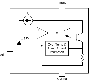
8.3 Feature Description
8.3.1 NPN Darlington Output Drive
NPN Darlington output topology provides naturally low output impedance and an output capacitor is optional. To support maximum current and lowest temperature, 2.5-V headroom is recommended (VI – VO).
8.3.2 Overload Block
Over-current and over-temperature shutdown protects the device against overload or damage from operating in excessive heat.
8.3.3 Programmable Feedback
Op amp with 1.25-V offset input at the ADJUST pin provides easy output voltage or current (not both) programming. For current regulation applications, a single resistor whose resistance value is 1.25 V / IOUT and power rating is greater than (1.25 V)2 / R should be used. For voltage regulation applications, two resistors set the output voltage. See Typical Application for a schematic and the resistor formula.
8.4 Device Functional Modes
8.4.1 Normal operation
The device OUTPUT pin will source current necessary to make OUTPUT pin 1.25 V greater than ADJUST terminal to provide output regulation.
8.4.2 Operation With Low Input Voltage
The device requires up to 2.5-V headroom (VI – VO) to operate in regulation. With less headroom, the device may drop out and OUTPUT voltage will be INPUT voltage minus drop out voltage.
8.4.3 Operation at Light Loads
The device passes its bias current to the OUTPUT pin. The load or feedback must consume this minimum current for regulation or the output may be too high.
8.4.4 Operation In Self Protection
When an overload occurs the device will shut down Darlington NPN output stage or reduce the output current to prevent device damage. The device will automatically reset from the overload. The output may be reduced or alternate between on and off until the overload is removed.