7 Specifications
7.1 Absolute Maximum Ratings
over operating free-air temperature range (unless otherwise noted) (1)(2)(3)
|
MIN |
MAX |
UNIT |
| VIN to GND |
–0.3 |
6 |
V |
| VSW, VOVP, VILED to GND |
|
45 |
| VSCL, VSDA, VALS1, VPWM, VINT, VHWEN to GND |
|
6 |
| VALS2 to GND |
–0.3 V to VIN + 0.3 V |
| Continuous power dissipation |
Internally limited |
| Junction temperature (TJ-MAX) |
|
150 |
°C |
| Maximum lead temperature (soldering, 10s) |
See(4) |
|
| Storage temperature, Tstg |
–65 |
150 |
°C |
(1) Stresses beyond those listed under Absolute Maximum Ratings may cause permanent damage to the device. These are stress ratings only, which do not imply functional operation of the device at these or any other conditions beyond those indicated under Recommended Operating Conditions. Exposure to absolute-maximum-rated conditions for extended periods may affect device reliability.
(2) If Military/Aerospace specified devices are required, please contact the Texas Instruments Sales Office/ Distributors for availability and specifications.
(3) All voltages are with respect to the potential at the GND pin.
(4) For detailed soldering specifications and information, please refer to Application Note 1112:
DSBGA Wafer Level Chip Scale Package (
SNVA009).
7.2 ESD Ratings
|
VALUE |
UNIT |
| V(ESD) |
Electrostatic discharge |
Human-body model (HBM), per ANSI/ESDA/JEDEC JS-001(1) |
±2000 |
V |
(1) JEDEC document JEP155 states that 500-V HBM allows safe manufacturing with a standard ESD control process.
7.3 Recommended Operating Conditions
over operating free-air temperature range (unless otherwise noted)
|
MIN |
NOM |
MAX |
UNIT |
| VIN to GND |
2.7 |
|
5.5 |
V |
| VSW, VOVP, VILED, to GND |
0 |
|
40 |
| Junction temperature (TJ)(1) |
–40 |
|
125 |
°C |
| Ambient temperature (TA)(2) |
–40 |
|
85 |
(1) Internal thermal shutdown circuitry protects the device from permanent damage. Thermal shutdown engages at TJ= 140°C (typ.) and disengages at TJ= 125°C (typ.).
(2) In applications where high power dissipation and/or poor package thermal resistance is present, the maximum ambient temperature may have to be derated. Maximum ambient temperature (TA-MAX) is dependent on the maximum operating junction temperature (TJ-MAX-OP = 125°C), the maximum power dissipation of the device in the application (PD-MAX), and the junction-to ambient thermal resistance of the part/package in the application (RθJA), as given by the following equation: TA-MAX = TJ-MAX-OP – (RθJA × PD-MAX).
7.4 Thermal Information
| THERMAL METRIC(1) |
DSBGA |
UNIT |
| YFQ |
YFZ |
| 12 PINS |
| RθJA |
Junction-to-ambient thermal resistance(2) |
61.7 |
°C/W |
(1) For more information about traditional and new thermal metrics, see the
IC Package Thermal Metrics application report,
SPRA953.
(2) Junction-to-ambient thermal resistance (RθJA) is taken from a thermal modeling result, performed under the conditions and guidelines set forth in the JEDEC standard JESD51-7. The test board is a 4-layer FR-4 board measuring 102 mm x 76 mm x 1.6 mm with a 2 x 1 array of thermal vias. The ground plane on the board is 50 mm x 50 mm. Thickness of copper layers are 36 µm/18 µm/18 µm/3 6µm (1.5oz/1oz/1oz/1.5oz). Ambient temperature in simulation is 22°C in still air. Power dissipation is 1W. The value of RθJA of this product in the DSBGA package could fall in a range as wide as 60ºC/W to 110ºC/W (if not wider), depending on PCB material, layout, and environmental conditions. In applications where high maximum power dissipation exists special care must be paid to thermal dissipation issues.
7.5 Electrical Characteristics
Typical (TYP) limits are for TA = 25°C; minimum (MIN) and maximum (MAX) apply over the full operating ambient temperature range (−40°C ≤ TA ≤ 85°C); VIN = 3.6 V, unless otherwise specified.(1)(2)
| PARAMETER |
TEST CONDITIONS |
MIN |
TYP |
MAX |
UNIT |
| ILED |
Output current regulation |
2.7 V ≥ VIN ≥ 5.5 V, Full-scale current = 19 mA, BRT Code = 0x7F, ALS Select Bit = 0, I2C Enable = 1 |
17.11 |
18.6 |
20.08 |
mA |
| VREG_CS |
Regulated current sink headroom voltage |
|
|
400 |
|
mV |
| VHR |
Current sink minimum headroom voltage |
ILED = 95% of nominal |
|
200 |
|
mV |
| RDSON |
NMOS switch on resistance |
ISW = 100 mA |
|
0.25 |
|
Ω |
| ICL |
NMOS switch current limit |
2.7 V ≤ VIN ≤ 5.5 V |
739 |
839 |
936 |
mA |
| VOVP |
Output overvoltage protection |
ON Threshold, 2.7 V ≤ VIN ≤ 5.5 V |
40-V version |
40 |
41 |
42 |
V |
| 25-V version |
23.6 |
24 |
24.6 |
| Hysteresis |
|
1 |
|
| fSW |
Switching frequency |
2.7 V ≤ VIN ≤ 5.5 V |
450 |
500 |
550 |
kHz |
| DMAX |
Maximum duty cycle |
|
|
94% |
|
|
| DMIN |
Minimum duty cycle |
|
|
10% |
|
|
| IQ |
Quiescent current, device not switching |
VHWEN = VIN |
|
490 |
600 |
µA |
| IQ_SW |
Switching supply current |
ILED = 19 mA, VOUT = 36 V |
|
1.35 |
|
mA |
| ISHDN |
Shutdown current |
VHWEN = GND, 2.7 V ≥ VIN ≥ 5.5 V |
|
1 |
2 |
µA |
| ILED_MIN |
Minimum LED current |
Full-scale current = 19 mA setting
BRT = 0x01 |
|
9.5 |
|
µA |
| VALS |
Ambient light sensor reference voltage |
2.7 V ≥ VIN ≥ 5.5 V (3) |
0.97 |
1 |
1.03 |
V |
| VHWEN |
Logic thresholds - logic low |
|
0 |
|
0.4 |
V |
| Logic thresholds - logic high |
|
1.2 |
|
VIN |
| TSD |
Thermal shutdown |
|
|
140 |
|
°C |
| Hysteresis |
|
|
15 |
|
| RALS1, RALS2 |
ALS input internal pull-down resistors |
2.7 V ≥ VIN ≥ 5.5 V |
12.77 |
13.531 |
14.29 |
kΩ |
| 8.504 |
9.011 |
9.518 |
| 5.107 |
5.411 |
5.715 |
| 2.143 |
2.271 |
2.399 |
| 1.836 |
1.946 |
2.055 |
| 1.713 |
1.815 |
1.917 |
| 1.510 |
1.6 |
1.69 |
| 1.074 |
1.138 |
1.202 |
| 0.991 |
1.050 |
1.109 |
| 0.954 |
1.011 |
1.068 |
| 0.888 |
0.941 |
0.994 |
| 0.717 |
0.759 |
0.802 |
| 0.679 |
0.719 |
0.760 |
| 0.661 |
0.700 |
0.740 |
| 0.629 |
0.666 |
0.704 |
| LOGIC VOLTAGE SPECIFICATIONS (SCL, SDA, PWM, INT) |
| VIL |
Input logic low |
2.7 V ≤ VIN ≤ 5.5 V |
0 |
|
0.54 |
V |
| VIH |
Input logic high |
2.7 V ≤ VIN ≤ 5.5 V |
1.26 |
|
VIN |
V |
| VOL |
Output logic low (SDA, INT) |
ILOAD = 3 mA |
|
|
400 |
mV |
(1) All voltages are with respect to the potential at the GND pin.
(2) Min and Max limits are verified by design, test, or statistical analysis. Typical (typ.) numbers are not verified, but represent the most likely norm.
(3) The ALS voltage specification is the maximum trip threshold for the ALS zone boundary (Code 0xFF). Due to random offsets and the mechanism for which the hysteresis voltage varies, it is recommended that only Codes 0x04 and above be used for Zone Boundary Thresholds. See
Zone Boundary Trip Points and Hysteresis and
Minimum Zone Boundary Settings sections.
7.6 I2C-Compatible Timing Requirements (SCL, SDA)(1)
|
MIN |
NOM |
MAX |
UNIT |
| t1 |
SCL (Clock Period) |
2.5 |
|
|
µs |
| t2 |
Data in setup time to SCL high |
100 |
|
|
ns |
| t3 |
Data out stable after SCL low |
0 |
|
|
ns |
| t4 |
SDA low setup time to SCL low (start) |
100 |
|
|
ns |
| t5 |
SDA high hold time after SCL High (stop) |
100 |
|
|
ns |
(1) SCL and SDA must be glitch-free in order for proper brightness control to be realized.
7.7 Simple Interface Timing
|
MIN |
NOM |
MAX |
UNIT |
| tPWM_HIGH |
Enable time, PWM pin must be held high |
1.5 |
2 |
2.6 |
ms |
| tPWM_LOW |
Disable time, PWM pin must be held low |
1.48 |
2 |
2.69 |
7.8 Typical Characteristics
VIN = 3.6 V, LEDs are OVSRWAC1R6 from OPTEK Technology, COUT = 1 µF, CIN = 1 µF, L = TDK VLF5012ST-100M1R0, (RL = 0.24 Ω), ILED = 19 mA, TA = 25°C, unless otherwise specified.
 Figure 3. LED Current vs VIN

| ALS Resistor Select Register = 0x44 |
|
|
|
|
Figure 5. Internal ALS Resistor vs VIN

| TA = −40°C |
ALS Resistor Select Register = 0x44 |
|
|
|
Figure 7. Internal ALS Resistor vs VIN
 Figure 9. Max Duty Cycle vs VIN
 Figure 11. Switching Frequency vs VIN
 Figure 13. Simple Disable Time vs VIN

| Channel 2: SDA (5V/div) |
Time Base (40ms/div) |
| Channel 3: ILED (10mA/div) |
|
| 1.024ms/Step Up And Down |
|
Figure 15. Ramp Rate (Exponential)

| Channel 2: SDA (5V/div) |
Time Base (200ms/div) |
| Channel 3: ILED (10mA/div) |
|
| 4.096ms/Step Up And Down |
|
Figure 17. Ramp Rate (Exponential)

| Channel 2: SDA (5V/div) |
Time Base (1s/div) |
| Channel 3: ILED (10mA/div) |
|
| 16.384ms/Step Up And Down |
|
Figure 19. Ramp Rate (Exponential)

| Channel 2: SDA (5V/div) |
Time Base (4s/div) |
| Channel 3: ILED (10mA/div) |
|
| 65.538ms/Step Up And Down |
|
|
|
Figure 21. Ramp Rate (Exponential)

| Channel 1: VIN (500mV/div) |
Time Base (400µs/div) |
| Channel 2: VOUT (500mV/div) |
L = 22 µH |
| Channel 3: ILED (500µA/div) |
ILED = 19 mA |
| VIN From 3.6 V To 3.2 V |
|
Figure 23. Line Step Response

|
Closed Loop |
|
L = 22 µH |
|
| The value for current limit given in the Electrical Characteristics is measured in an open loop test by forcing current into SW until the current limit comparator threshold is reached. The typical curve for current limit is measured in closed loop using the typical application circuit by increasing IOUT until the peak inductor current stops increasing. Closed loop data appears higher due to the delay between the comparator trip point and the NFET turning off. This delay allows the closed loop inductor current to ramp higher after the trip point by approximately 100 ns × VIN/L. |
Figure 25. Current Limit vs VIN
 Figure 4. Shutdown Current vs VIN

| TA = 85°C |
ALS Resistor Select Register = 0x44 |
|
|
|
Figure 6. Internal ALS Resistor vs VIN
 Figure 8. Overvoltage Protection vs VIN
 Figure 10. NFET Switch On-Resistance vs VIN
 Figure 12. Simple Enable Time vs VIN

| ILED Full Scale = 19 mA |
50% Duty Cycle |
|
|
|
|
Figure 14. ILED vs FPWM

| Channel 2: SDA (5V/div) |
Time Base (100ms/div) |
| Channel 3: ILED (10mA/div) |
|
| 2.048ms/Step Up And Down |
|
Figure 16. Ramp Rate (Exponential)

| Channel 2: SDA (5V/div) |
Time Base (400ms/div) |
| Channel 3: ILED (10mA/div) |
|
| 8.192ms/Step Up And Down |
|
Figure 18. Ramp Rate (Exponential)

| Channel 2: SDA (5V/div) |
Time Base (2s/div) |
| Channel 3: ILED (10mA/div) |
|
| 32.768ms/Step Up And Down |
|
Figure 20. Ramp Rate (Exponential)

| Channel 1: IIN (200mA/div) |
Time Base (2ms/div) |
| Channel 3: VOUT (20V/div) |
Ramp Rate = 8µs/Step |
| Channel 4 (10mA/div) |
ILED = 19mA |
| L = 22 µH |
VIN = 3.6V |
|
Figure 22. Start-up Plot

| Channel 2: PWM (5V/div) |
Time Base (2ms/div) |
|
| Channel 4: ILED (5mA/div) |
ILED Full Scale = 19 mA |
|
| DPWM From 30% To 70% |
FPWM = 5 kHz |
|
|
|
|
Figure 24. ILED Response To Step Change In PWM Duty Cycle
 Figure 1. I2C-Compatible Timing
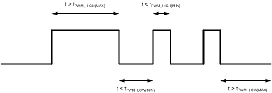 Figure 2. Simple Enable/Disable Timing