JAJSAQ4F January 2007 – May 2021 LM5002
PRODUCTION DATA
- 1 特長
- 2 アプリケーション
- 3 概要
- 4 Revision History
- 5 Pin Configuration and Functions
- 6 Specifications
- 7 Detailed Description
- 8 Application and Implementation
- 9 Power Supply Recommendations
- 10Layout
- 11Device and Documentation Support
- 12Mechanical, Packaging, and Orderable Information
パッケージ・オプション
メカニカル・データ(パッケージ|ピン)
サーマルパッド・メカニカル・データ
発注情報
8.2.1.2.7 Loop Compensation
The loop bandwidth and phase margin determines the response to load transients, while ensuring that the output noise level meets the requirements. A common choice of loop unity gain frequency is 5% of the switching frequency. This is simple to compensate, low noise and provides sufficient transient response for most applications. The plant bode plot is examined for gain and phase at the desired loop unity-gain frequency and the compensator is designed to adjust the loop gain and phase to meet the intended loop unity gain frequency and phase margin (typically about 55°). When gain is required, the ratio of RCOMP and RFB_TOP sets the error amplifier to provide the correct amount.
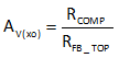
where (in reference to Figure 8-5):
- RCOMP is R4
- RFB_TOP is R5
The phase margin is boosted by a transfer function zero at frequency given by Equation 23 and a pole at frequency given by Equation 24.
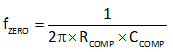
where (in reference to ):
- CCOMP is C6
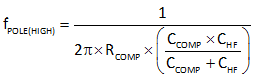
where (in reference to Figure 8-5):
- CHF is C5
The low frequency pole is determined with Equation 26.
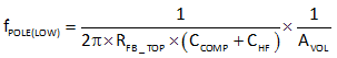
where (in reference to Figure 8-5):
- AVOL is the open loop gain of the error amplifier
Optimal regulation is achieved by setting FPOLE(LOW) as high as possible, but still permitting FZERO to insure the desired phase margin. The feedback resistors (RFB_TOP and RFB_BOTTOM) are chosen to be 10.2 kΩ and 3.4 kΩ respectively. These values produce a feedback signal that has a desirable signal to noise ratio. FZERO and FPOLE(HIGH) are set to be 450 Hz and 25.5 kHz respectively. Based on these values, RCOMP, CCOMP, and CHF are chosen to be 7.5 kΩ, 0.47 µF, and 820 pF respectively. These values produce a crossover frequency of approximately 3 kHz with a phase margin of 60°.