JAJSLR9I February 2006 – May 2021 LM5009
PRODUCTION DATA
- 1 特長
- 2 アプリケーション
- 3 概要
- 4 Revision History
- 5 Pin Configuration and Functions
- 6 Specifications
- 7 Detailed Description
-
8 Application and Implementation
- 8.1 Application Information
- 8.2
Typical Application
- 8.2.1 Design Requirements
- 8.2.2
Detailed Design Procedure
- 8.2.2.1 Output Resistor Divider Selection
- 8.2.2.2 Frequency Selection
- 8.2.2.3 Inductor Selection
- 8.2.2.4 VCC and Bootstrap Capacitor
- 8.2.2.5 Output Capacitor Selection
- 8.2.2.6 Current Limit Off-Timer Setting
- 8.2.2.7 Rectifier Diode Selection
- 8.2.2.8 Input Capacitor Selection
- 8.2.2.9 Ripple Configuration
- 8.2.3 Application Curves
- 8.3 Do's and Don'ts
- 9 Power Supply Recommendations
- 10Layout
- 11Device and Documentation Support
- 12Mechanical, Packaging, and Orderable Information
パッケージ・オプション
メカニカル・データ(パッケージ|ピン)
サーマルパッド・メカニカル・データ
発注情報
8.2.2.3 Inductor Selection
L1: The main parameter affected by the inductor is the output current ripple amplitude. The choice of inductor value therefore depends on both the minimum and maximum load currents, keeping in mind that the maximum ripple current occurs at maximum VIN.
- Minimum load current: To maintain continuous conduction at minimum IO (100 mA), the ripple amplitude (IOR) must be less than 200 mA peak-to-peak so the lower peak of the waveform does not reach zero. L1 is calculated using Equation 7:
Equation 7.
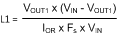
At VIN = 90 V, L1 (min) calculates to 132 µH. The next larger standard value (150 µH) is chosen and, with this value, IOR calculates to 176 mA peak-to-peak at VIN = 90 V and 33 mA peak-to-peak at VIN = 12 V.
- Maximum load current: At a load current of 150 mA, the peak of the ripple waveform must not reach the minimum value of the LM5009 current limit threshold (250 mA). Therefore, the ripple amplitude must be less than 200 mA peak-to-peak, which is already satisfied in Equation 7. With L1 = 150 µH, at maximum VIN and IO, the peak of the ripple is 238 mA. Although L1 must carry this peak current without saturating or exceeding its temperature rating, L1 must also be capable of carrying the maximum value of the LM5009 current limit threshold (370 mA) without saturating because the current limit is reached during startup.