JAJSLR9I February 2006 – May 2021 LM5009
PRODUCTION DATA
- 1 特長
- 2 アプリケーション
- 3 概要
- 4 Revision History
- 5 Pin Configuration and Functions
- 6 Specifications
- 7 Detailed Description
-
8 Application and Implementation
- 8.1 Application Information
- 8.2
Typical Application
- 8.2.1 Design Requirements
- 8.2.2
Detailed Design Procedure
- 8.2.2.1 Output Resistor Divider Selection
- 8.2.2.2 Frequency Selection
- 8.2.2.3 Inductor Selection
- 8.2.2.4 VCC and Bootstrap Capacitor
- 8.2.2.5 Output Capacitor Selection
- 8.2.2.6 Current Limit Off-Timer Setting
- 8.2.2.7 Rectifier Diode Selection
- 8.2.2.8 Input Capacitor Selection
- 8.2.2.9 Ripple Configuration
- 8.2.3 Application Curves
- 8.3 Do's and Don'ts
- 9 Power Supply Recommendations
- 10Layout
- 11Device and Documentation Support
- 12Mechanical, Packaging, and Orderable Information
パッケージ・オプション
メカニカル・データ(パッケージ|ピン)
サーマルパッド・メカニカル・データ
発注情報
7.3.2 High Voltage Startup Regulator
The LM5009 contains an internal high voltage startup regulator. The input pin (VIN) can be connected directly to line voltages up to 95 V, with transient capability to 100 V. The regulator is internally current limited at 9.5 mA. Upon power-up, the regulator sources current into the external capacitor at VCC (C3). When the voltage on the VCC pin reaches the undervoltage lockout threshold of 6.3 V, the buck switch is enabled.
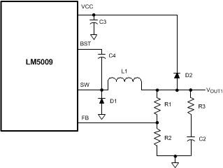
In applications involving a high value for VIN, where power dissipation in the VCC regulator is a concern, an auxiliary voltage can be diode connected to the VCC pin. Setting the voltage between 8 V and 14 V shuts off the internal regulator, reducing internal power dissipation, as shown in Figure 7-2. The current required into the VCC pin is illustrated in the Section 6.6 section.
 Figure 7-2 Self-Biased Configuration