JAJSLR9I February 2006 – May 2021 LM5009
PRODUCTION DATA
- 1 特長
- 2 アプリケーション
- 3 概要
- 4 Revision History
- 5 Pin Configuration and Functions
- 6 Specifications
- 7 Detailed Description
-
8 Application and Implementation
- 8.1 Application Information
- 8.2
Typical Application
- 8.2.1 Design Requirements
- 8.2.2
Detailed Design Procedure
- 8.2.2.1 Output Resistor Divider Selection
- 8.2.2.2 Frequency Selection
- 8.2.2.3 Inductor Selection
- 8.2.2.4 VCC and Bootstrap Capacitor
- 8.2.2.5 Output Capacitor Selection
- 8.2.2.6 Current Limit Off-Timer Setting
- 8.2.2.7 Rectifier Diode Selection
- 8.2.2.8 Input Capacitor Selection
- 8.2.2.9 Ripple Configuration
- 8.2.3 Application Curves
- 8.3 Do's and Don'ts
- 9 Power Supply Recommendations
- 10Layout
- 11Device and Documentation Support
- 12Mechanical, Packaging, and Orderable Information
パッケージ・オプション
メカニカル・データ(パッケージ|ピン)
サーマルパッド・メカニカル・データ
発注情報
7.3.1 Control Circuit Overview
The LM5009 is a buck dc-dc regulator that uses a control scheme where the on-time varies inversely with line voltage (VIN). Control is based on a comparator and the on-time one-shot, with the output voltage feedback (FB) compared to an internal reference (2.5 V). If the FB level is below the reference, then the buck switch is turned on for a fixed time determined by the line voltage and a programming resistor (RON). Following the on period, the switch remains off for at least the minimum off-timer period of 300 ns. If FB is still below the reference at that time, then the switch turns on again for another on-time period. This cycle continues until regulation is achieved, at which time the off-time increases based on the required duty cycle.
The LM5009 operates in discontinuous conduction mode at light load currents, and continuous conduction mode at heavy load current. In discontinuous conduction mode, current through the output inductor starts at zero and ramps up to a peak during the on-time, then ramps back to zero before the end of the off-time. The next on-time period starts when the voltage at FB falls below the internal reference—until then, the inductor current remains zero. In this mode the operating frequency is lower than in continuous conduction mode, and varies with load current. Therefore, at light loads the conversion efficiency is maintained because the switching losses reduce with the reduction in load and frequency. The discontinuous operating frequency can be calculated as by Equation 1:
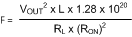
where
- RL = the load resistance
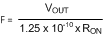
In continuous conduction mode, current flows continuously through the inductor and never ramps down to zero. In this mode, the operating frequency is greater than the discontinuous mode frequency and remains relatively constant with load and line variations. The approximate continuous mode operating frequency can be calculated by Equation 2:
The output voltage (VOUT) is programmed by two external resistors; see the Section 7.2 section. The regulation point is calculated by Equation 3:
This regulator regulates the output voltage based on ripple voltage at the feedback input, requiring a minimum amount of equivalent series resistance (ESR) for the output capacitor C2. A minimum of 25 mV of ripple voltage at the feedback pin (FB) is required for the LM5009. In cases where the capacitor ESR is too small, additional series resistance may be required (see R3 in the Section 7.2 section).
For applications where lower output voltage ripple is required, the output can be taken directly from a low-ESR output capacitor, as shown in Figure 7-1. However, R3 slightly degrades the load regulation.
 Figure 7-1 Low Ripple Output Configuration