JAJSLR9I February 2006 – May 2021 LM5009
PRODUCTION DATA
- 1 特長
- 2 アプリケーション
- 3 概要
- 4 Revision History
- 5 Pin Configuration and Functions
- 6 Specifications
- 7 Detailed Description
-
8 Application and Implementation
- 8.1 Application Information
- 8.2
Typical Application
- 8.2.1 Design Requirements
- 8.2.2
Detailed Design Procedure
- 8.2.2.1 Output Resistor Divider Selection
- 8.2.2.2 Frequency Selection
- 8.2.2.3 Inductor Selection
- 8.2.2.4 VCC and Bootstrap Capacitor
- 8.2.2.5 Output Capacitor Selection
- 8.2.2.6 Current Limit Off-Timer Setting
- 8.2.2.7 Rectifier Diode Selection
- 8.2.2.8 Input Capacitor Selection
- 8.2.2.9 Ripple Configuration
- 8.2.3 Application Curves
- 8.3 Do's and Don'ts
- 9 Power Supply Recommendations
- 10Layout
- 11Device and Documentation Support
- 12Mechanical, Packaging, and Orderable Information
パッケージ・オプション
メカニカル・データ(パッケージ|ピン)
サーマルパッド・メカニカル・データ
発注情報
8.2.2.8 Input Capacitor Selection
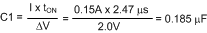
C1: The purpose of this capacitor is to supply most of the switch current during the on-time and to limit the voltage ripple at VIN, on the assumption that the voltage source feeding VIN has an output impedance greater than zero. At maximum load current, when the buck switch turns on, the current into pin 8 suddenly increases to the lower peak of the output current waveform, ramps up to the peak value, and then drops to zero at turn-off. The average input current during this on-time is the load current (150 mA). For a worst-case calculation, C1 must supply this average load current during the maximum on-time. To keep the input voltage ripple to less than 2 V (for this exercise), C1 calculates to Equation 11:
Quality ceramic capacitors in this value have a low ESR that adds only a few millivolts to the ripple. The capacitance is dominant in this case. To allow for the capacitor tolerance, temperature effects, and voltage effects, a 1.0-µF, 100-V, X7R capacitor is used.
C5: This capacitor helps avoid supply voltage transients and ringing resulting from long lead inductance at VIN. A low-ESR, 0.1-µF ceramic chip capacitor is recommended, located close to the LM5009.