SNVS424D January 2006 – December 2014 LM5106
PRODUCTION DATA.
- 1 Features
- 2 Applications
- 3 Description
- 4 Revision History
- 5 Pin Configuration and Functions
- 6 Specifications
- 7 Detailed Description
- 8 Application and Implementation
- 9 Power Supply Recommendations
- 10Layout
- 11Device and Documentation Support
- 12Mechanical, Packaging, and Orderable Information
パッケージ・オプション
メカニカル・データ(パッケージ|ピン)
サーマルパッド・メカニカル・データ
- DPR|10
発注情報
1 Features
- Drives Both a High-Side and Low-Side N-Channel MOSFET
- 1.8-A Peak Output Sink Current
- 1.2-A Peak Output Source Current
- Bootstrap Supply Voltage Range up to 118-V DC
- Single TTL Compatible Input
- Programmable Turnon Delays (Dead-Time)
- Enable Input Pin
- Fast Turnoff Propagation Delays (32 ns Typical)
- Drives 1000 pF With 15-ns Rise and 10-ns Fall Time
- Supply Rail Undervoltage Lockout
- Low Power Consumption
- 10-Pin WSON Package (4 mm × 4 mm) and 10-Pin VSSOP Package
2 Applications
- Solid-State Motor Drives
- Half-Bridge and Full-Bridge Power Converters
- Two Switch Forward Power Converters
3 Description
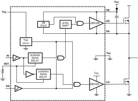
The LM5106 is a high-voltage gate driver designed to drive both the high-side and low-side N-channel MOSFETs in a synchronous buck or half-bridge configuration. The floating high-side driver can work with rail voltages up to 100 V. The single control input is compatible with TTL signal levels and a single external resistor programs the switching transition dead-time through tightly matched turnon delay circuits. The robust level shift technology operates at high speed while consuming low power and provides clean output transitions. Undervoltage lockout (UVLO) disables the gate driver when either the low side or the bootstrapped high-side supply voltage is below the operating threshold. The LM5106 is offered in the 10-pin VSSOP or the thermally enhanced 10-pin WSON plastic package.
Device Information(1)
| PART NUMBER | PACKAGE | BODY SIZE (NOM) |
|---|---|---|
| LM5106 | VSSOP (10) | 3.00 mm × 3.00 mm |
| WSON (10) | 4.00 mm × 4.00 mm |
- For all available packages, see the orderable addendum at the end of the datasheet.
Simplified Block Diagram