JAJSDX2C September 2017 – October 2021 LM5150-Q1
PRODUCTION DATA
- 1 特長
- 2 アプリケーション
- 3 概要
- 4 Revision History
- 5 Device Comparison Table
- 6 Pin Configuration and Functions
- 7 Specifications
-
8 Detailed Description
- 8.1 Overview
- 8.2 Functional Block Diagram
- 8.3
Feature Description
- 8.3.1 Enable (EN Pin)
- 8.3.2 High Voltage VCC Regulator (PVCC, AVCC Pin)
- 8.3.3 Power-On Voltage Selection (VSET Pin)
- 8.3.4 Switching Frequency (RT Pin)
- 8.3.5 Clock Synchronization (SYNC Pin in SS Configuration)
- 8.3.6 Current Sense, Slope Compensation, and PWM (CS Pin)
- 8.3.7 Current Limit (CS Pin)
- 8.3.8 Feedback and Error Amplifier (COMP Pin)
- 8.3.9 Automatic Wake-Up and Standby
- 8.3.10 Boost Status Indicator (STATUS Pin)
- 8.3.11 Maximum Duty Cycle Limit, Minimum Input Supply Voltage
- 8.3.12 MOSFET Driver (LO Pin)
- 8.3.13 Thermal Shutdown
- 8.4 Device Functional Modes
-
9 Application and Implementation
- 9.1 Application Information
- 9.2
Typical Application
- 9.2.1 Design Requirements
- 9.2.2
Detailed Design Procedure
- 9.2.2.1 Custom Design With WEBENCH® Tools
- 9.2.2.2 RSET Resistor
- 9.2.2.3 RT Resistor
- 9.2.2.4 Inductor Selection (LM)
- 9.2.2.5 Current Sense (RS)
- 9.2.2.6 Slope Compensation Ramp (RSL)
- 9.2.2.7 Output Capacitor (COUT)
- 9.2.2.8 Loop Compensation Component Selection and Maximum ESR
- 9.2.2.9 PVCC Capacitor, AVCC Capacitor, and AVCC Resistor
- 9.2.2.10 VOUT Filter (CVOUT, RVOUT)
- 9.2.2.11 Input Capacitor
- 9.2.2.12 MOSFET Selection
- 9.2.2.13 Diode Selection
- 9.2.2.14 Efficiency Estimation
- 9.2.3 Application Curves
- 9.3 System Examples
- 10Power Supply Recommendations
- 11Layout
- 12Device and Documentation Support
- 13Mechanical, Packaging, and Orderable Information
パッケージ・オプション
デバイスごとのパッケージ図は、PDF版データシートをご参照ください。
メカニカル・データ(パッケージ|ピン)
- RUM|16
サーマルパッド・メカニカル・データ
発注情報
9.1.2 Loop Response
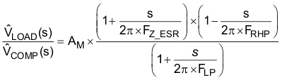
The open-loop transfer function of a boost regulator is defined as the product of modulator transfer function and feedback transfer function.
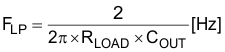
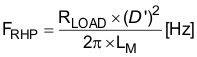
The modulator transfer function of a current mode boost regulator including a power stage with an embedded current loop can be simplified as a one load pole (FLP), one ESR zero (FZ_ESR), and one Right Half Plane (RHP) zero (FRHP) system, which can be explained as follows.
Modulator transfer function is defined as follows:
where
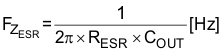
RESR is the equivalent series resistance (ESR) of the output capacitor which is specified in the capacitor data sheet.
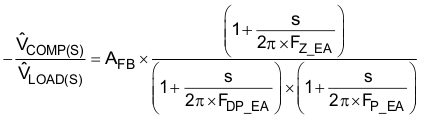
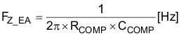
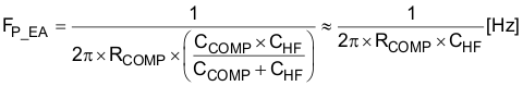
RCOMP, CCOMP, and CHF (see Figure 9-3) configure the error amplifier gain and phase characteristics to produce a stable voltage loop with fast response. This compensation network creates a dominant pole at low frequency (FDP_EA), a mid-band zero (FZ_EA), and a high frequency pole (FP_EA).
The feedback transfer function is defined as follows:
where
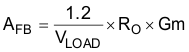
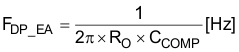
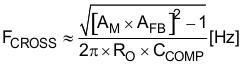
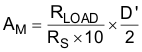
RO (≈ 10 MΩ) is the output resistance of the error amplifier and Gm (≈ 2 mA/V) is the transconductance of the error amplifier.
Assuming FLP is canceled by FZ_EA, FRHP is much higher than crossover frequency (FCROSS), and FZ_ESR is either canceled by FP_EA or FZ_ESR is much higher than FCROSS, the open-loop transfer function can be simplified as follows:
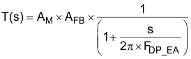
Because |T(s)| = 1 at the crossover frequency, the crossover frequency can be simply estimated using those assumptions.