JAJSDX2C September 2017 – October 2021 LM5150-Q1
PRODUCTION DATA
- 1 特長
- 2 アプリケーション
- 3 概要
- 4 Revision History
- 5 Device Comparison Table
- 6 Pin Configuration and Functions
- 7 Specifications
-
8 Detailed Description
- 8.1 Overview
- 8.2 Functional Block Diagram
- 8.3
Feature Description
- 8.3.1 Enable (EN Pin)
- 8.3.2 High Voltage VCC Regulator (PVCC, AVCC Pin)
- 8.3.3 Power-On Voltage Selection (VSET Pin)
- 8.3.4 Switching Frequency (RT Pin)
- 8.3.5 Clock Synchronization (SYNC Pin in SS Configuration)
- 8.3.6 Current Sense, Slope Compensation, and PWM (CS Pin)
- 8.3.7 Current Limit (CS Pin)
- 8.3.8 Feedback and Error Amplifier (COMP Pin)
- 8.3.9 Automatic Wake-Up and Standby
- 8.3.10 Boost Status Indicator (STATUS Pin)
- 8.3.11 Maximum Duty Cycle Limit, Minimum Input Supply Voltage
- 8.3.12 MOSFET Driver (LO Pin)
- 8.3.13 Thermal Shutdown
- 8.4 Device Functional Modes
-
9 Application and Implementation
- 9.1 Application Information
- 9.2
Typical Application
- 9.2.1 Design Requirements
- 9.2.2
Detailed Design Procedure
- 9.2.2.1 Custom Design With WEBENCH® Tools
- 9.2.2.2 RSET Resistor
- 9.2.2.3 RT Resistor
- 9.2.2.4 Inductor Selection (LM)
- 9.2.2.5 Current Sense (RS)
- 9.2.2.6 Slope Compensation Ramp (RSL)
- 9.2.2.7 Output Capacitor (COUT)
- 9.2.2.8 Loop Compensation Component Selection and Maximum ESR
- 9.2.2.9 PVCC Capacitor, AVCC Capacitor, and AVCC Resistor
- 9.2.2.10 VOUT Filter (CVOUT, RVOUT)
- 9.2.2.11 Input Capacitor
- 9.2.2.12 MOSFET Selection
- 9.2.2.13 Diode Selection
- 9.2.2.14 Efficiency Estimation
- 9.2.3 Application Curves
- 9.3 System Examples
- 10Power Supply Recommendations
- 11Layout
- 12Device and Documentation Support
- 13Mechanical, Packaging, and Orderable Information
パッケージ・オプション
デバイスごとのパッケージ図は、PDF版データシートをご参照ください。
メカニカル・データ(パッケージ|ピン)
- RUM|16
サーマルパッド・メカニカル・データ
発注情報
8.3.6 Current Sense, Slope Compensation, and PWM (CS Pin)
The LM5150-Q1 features a low-side current sense amplifier with a gain of 10, and provides an internal slope compensation ramp to prevent subharmonic oscillation at high duty cycle. The device generates the slope compensation ramp using a sawtooth current source with a slope of 30 µA × FSW (typical). This current flows through an internal 2-kΩ resistor and out of the CS pin. The slope compensation ramp is determined by the RT resistor and is 60 mV × FSW (typical) at the input of the current sense amplifier and 600 mV × FSW (typical) at the output of the current sense amplifier. The slope compensation ramp can be increased by adding an external slope resistor (RSL) between the sense resistor (RS) and the CS pin, but take extra care when using RSL, because the peak current limit is affected by adding RSL. See Section 8.3.7 for more detailed information.
 Figure 8-2 Current Sensing and Slope Compensation
According to peak current mode control theory, the slope of the compensation ramp must be greater than half of the sensed inductor current falling slope to prevent subharmonic oscillation at high duty cycle. Therefore, the minimum amount of slope compensation should satisfy the following inequality:

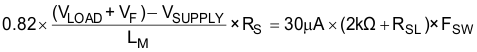
VF is a forward voltage drop of D1, the external diode. 1.2 is recommended as a margin to cover non-ideal factors.
If required, RSL can be added to increase the slope of the compensation ramp from half to 82% of the slope of the sensed inductor current during the falling slope. The typical RSL value is calculated using Equation 5. The maximum RSL value is 1 kΩ
The PWM comparator in Figure 8-2 compares the sum of sensed inductor current, the slope compensation ramp, and a 0.3-V (typical) internal COMP-to-PWM offset with the COMP pin voltage (VCOMP), and terminates the present cycle if the sum is greater than VCOMP.