JAJSKQ3D February   2016  – December 2022 LM5165

PRODUCTION DATA  

  1. 特長
  2. アプリケーション
  3. 概要
  4. Revision History
  5. Pin Configuration and Functions
  6. Specifications
    1. 6.1 Absolute Maximum Ratings
    2. 6.2 ESD Ratings
    3. 6.3 Recommended Operating Conditions
    4. 6.4 Thermal Information
    5. 6.5 Electrical Characteristics
    6. 6.6 Switching Characteristics
    7. 6.7 Typical Characteristics
  7. Detailed Description
    1. 7.1 Overview
    2. 7.2 Functional Block Diagram
    3. 7.3 Feature Description
      1. 7.3.1  Integrated Power MOSFETs
      2. 7.3.2  Selectable PFM or COT Mode Converter Operation
      3. 7.3.3  COT Mode Light-Load Operation
      4. 7.3.4  Low Dropout Operation and 100% Duty Cycle Mode
      5. 7.3.5  Adjustable Output Voltage (FB)
      6. 7.3.6  Adjustable Current Limit
      7. 7.3.7  Precision Enable (EN) and Hysteresis (HYS)
      8. 7.3.8  Power Good (PGOOD)
      9. 7.3.9  Configurable Soft Start (SS)
      10. 7.3.10 Thermal Shutdown
    4. 7.4 Device Functional Modes
      1. 7.4.1 Shutdown Mode
      2. 7.4.2 Standby Mode
      3. 7.4.3 Active Mode in COT
      4. 7.4.4 Active Mode in PFM
      5. 7.4.5 Sleep Mode in PFM
  8. Applications and Implementation
    1. 8.1 Application Information
    2. 8.2 Typical Applications
      1. 8.2.1 Design 1: Wide VIN, Low IQ COT Converter Rated at 5 V, 150 mA
        1. 8.2.1.1 Design Requirements
        2. 8.2.1.2 Detailed Design Procedure
          1. 8.2.1.2.1 Custom Design With WEBENCH® Tools
          2. 8.2.1.2.2 Switching Frequency – RT
          3. 8.2.1.2.3 Filter Inductor – LF
          4. 8.2.1.2.4 Output Capacitors – COUT
          5. 8.2.1.2.5 Series Ripple Resistor – RESR
          6. 8.2.1.2.6 Input Capacitor – CIN
          7. 8.2.1.2.7 Soft-Start Capacitor – CSS
        3. 8.2.1.3 Application Curves
      2. 8.2.2 Design 2: Small Solution Size PFM Converter Rated at 3.3 V, 50 mA
        1. 8.2.2.1 Design Requirements
        2. 8.2.2.2 Detailed Design Procedure
          1. 8.2.2.2.1 Peak Current Limit Setting – RILIM
          2. 8.2.2.2.2 Switching Frequency – LF
          3. 8.2.2.2.3 Output Capacitor – COUT
          4. 8.2.2.2.4 Input Capacitor – CIN
        3. 8.2.2.3 Application Curves
      3. 8.2.3 Design 3: High Density 12-V, 75-mA PFM Converter
        1. 8.2.3.1 Design Requirements
        2. 8.2.3.2 Detailed Design Procedure
          1. 8.2.3.2.1 Peak Current Limit Setting – RILIM
          2. 8.2.3.2.2 Switching Frequency – LF
          3. 8.2.3.2.3 Input and Output Capacitors – CIN, COUT
          4. 8.2.3.2.4 Feedback Resistors – RFB1, RFB2
          5. 8.2.3.2.5 Undervoltage Lockout Setpoint – RUV1, RUV2, RHYS
          6. 8.2.3.2.6 Soft Start – CSS
        3. 8.2.3.3 Application Curves
      4. 8.2.4 Design 4: 3.3-V, 150-mA COT Converter With High Efficiency
        1. 8.2.4.1 Design Requirements
        2. 8.2.4.2 Application Curves
      5. 8.2.5 Design 5: 15-V, 150-mA, 600-kHz COT Converter
        1. 8.2.5.1 Design Requirements
        2. 8.2.5.2 Detailed Design Procedure
          1. 8.2.5.2.1 COT Output Ripple Voltage Reduction
        3. 8.2.5.3 Application Curves
    3. 8.3 Power Supply Recommendations
    4. 8.4 Layout
      1. 8.4.1 Layout Guidelines
        1. 8.4.1.1 Compact PCB Layout for EMI Reduction
        2. 8.4.1.2 Feedback Resistor Layout
      2. 8.4.2 Layout Example
  9. Device and Documentation Support
    1. 9.1 Device Support
      1. 9.1.1 Third-Party Products Disclaimer
      2. 9.1.2 Development Support
      3. 9.1.3 Custom Design With WEBENCH® Tools
    2. 9.2 Documentation Support
      1. 9.2.1 Related Documentation
    3. 9.3 ドキュメントの更新通知を受け取る方法
    4. 9.4 サポート・リソース
    5. 9.5 Trademarks
    6. 9.6 静電気放電に関する注意事項
    7. 9.7 用語集
  10. 10Mechanical, Packaging, and Orderable Information

パッケージ・オプション

メカニカル・データ(パッケージ|ピン)
サーマルパッド・メカニカル・データ
発注情報

Typical Characteristics

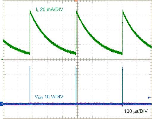
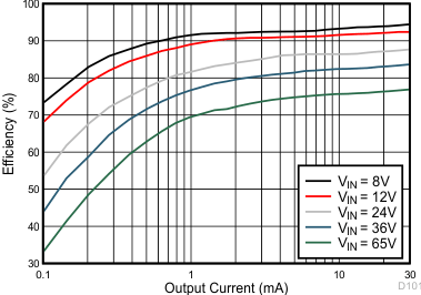
Unless otherwise specified, VIN = 12 V, VOUT = 5 V. Please refer to Typical Applications for circuit designs.
GUID-F220E884-FC3E-40AA-A7C4-C09AF9E24D79-low.gif
5-V, 25-mA Design LF = 470 µH
COUT = 47 µF
FSW(nom) = 100 kHz RILIM ≥ 100 kΩ
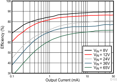
Figure 6-1 Converter Efficiency: 5 V, 25 mA, PFM
GUID-FD9D7434-439E-4AA0-AB17-85AEEC298F68-low.gif
See schematic,
Figure 8-14
LF = 47 µH
COUT = 10 µF
FSW(nom) = 350 kHz RILIM = 56.2 kΩ
Figure 6-3 Converter Efficiency: 3.3 V, 50 mA, PFM
GUID-D0D3C4FB-3C6B-4F8C-9EF4-E1450332B219-low.gif
See schematic,
Figure 8-21
LF = 47 µH
COUT = 10 µF
FSW(nom) = 500 kHz RILIM = 24.9 kΩ
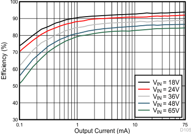
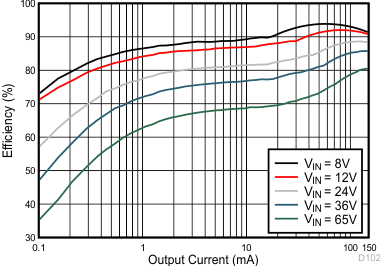
Figure 6-5 Converter Efficiency: 12 V, 75 mA, PFM
GUID-E56C3714-1CCB-49CA-A11A-0782A92243B5-low.gif
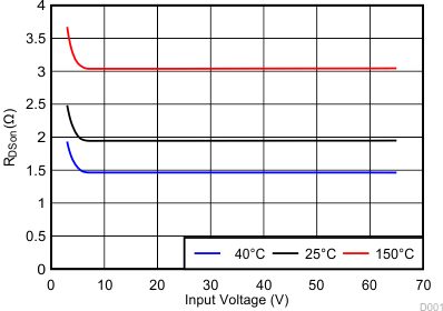
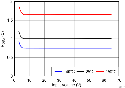
Figure 6-7 High-Side MOSFET On-State Resistance vs Input Voltage
GUID-E51B6C56-9BD6-4ECD-96F6-AD8D3D169348-low.gif
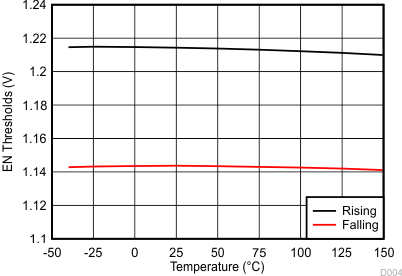
Figure 6-9 Enable Threshold Voltage vs Temperature
GUID-89C5B3EC-34C1-4A14-8249-0DC7CFE1F24C-low.gif
LM5165X
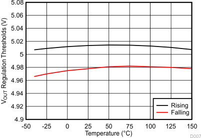
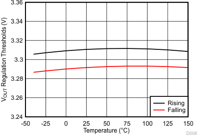
Figure 6-11 VOUT Regulation Thresholds vs Temperature
GUID-E7F25B90-E86C-4C07-BE8B-5002B87283F0-low.gif
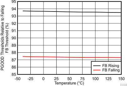
Figure 6-13 PGOOD Thresholds vs Temperature
GUID-75A1400D-7226-474F-B141-489B388530B4-low.gif
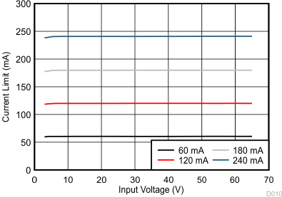
Figure 6-15 Peak Current Limits vs Input Voltage
GUID-86F9051A-A146-454B-B271-7BBCB7A9D0E9-low.gif
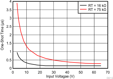
Figure 6-17 COT One-Shot Timer TON vs Input Voltage
GUID-A6BFDE34-58CE-4EE3-9D69-507F1F3E66E7-low.gif
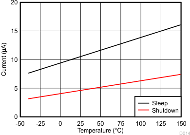
Figure 6-19 VIN Sleep and Shutdown Supply Current vs Temperature
GUID-2150F0CB-F1A2-41E1-ABA8-057B550E0B30-low.gif
RRT = 75 kΩ
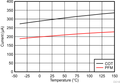
Figure 6-21 VIN Active Mode Supply Current vs Temperature
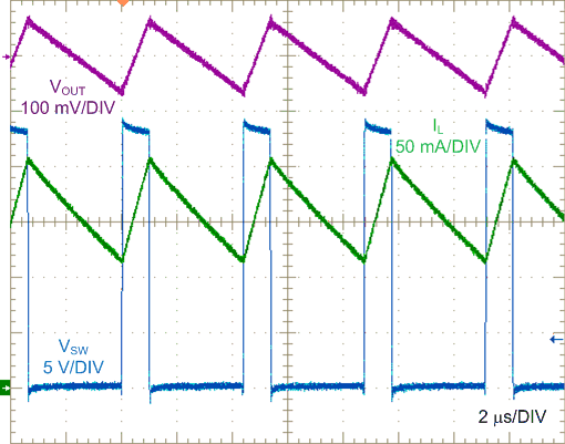
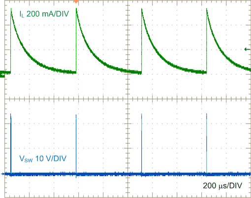
GUID-EA53B1C3-8D12-4175-92C3-50C130965629-low.gifFigure 6-23 Full Load Switching Waveforms, COT
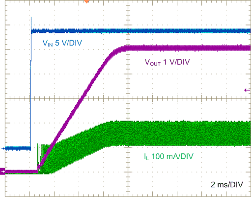
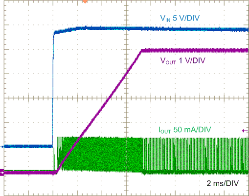
GUID-4AA5350B-F711-4D44-93AF-05C5142574F4-low.gifFigure 6-25 Full Load Start-Up, COT
GUID-AC354F11-54F3-4A35-8E10-BA5716280176-low.gifFigure 6-27 Full Load Switching Waveforms, PFM
GUID-D75AC62A-3C12-47E5-B633-D662D06529D6-low.gifFigure 6-29 Full Load Start-Up, PFM
GUID-393AB546-9306-4D2D-ABBA-900295CFA2CD-low.gif
See schematic,
Figure 8-1
LF = 220 µH
COUT = 22 µF
FSW(nom) = 230 kHz RRT = 133 kΩ
Figure 6-2 Converter Efficiency: 5 V, 150 mA, COT
GUID-403C4C04-70F8-4FB9-A70F-0B2C1F3C3F96-low.gif
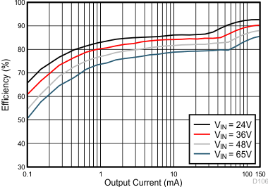
See schematic,
Figure 8-26
LF = 150 µH
COUT = 22 µF
FSW(nom) = 160 kHz RRT = 121 kΩ
Figure 6-4 Converter Efficiency: 3.3 V, 150 mA, COT
GUID-3B39A975-8EE4-4D3F-9390-15F93A9CEF51-low.gif
See schematic,
Figure 8-29
LF = 150 µH
COUT = 10 µF
FSW(nom) = 600 kHz RRT = 143 kΩ
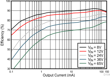
Figure 6-6 Converter Efficiency: 15 V, 150 mA, COT
GUID-3F29F955-0232-4EA5-85A8-A16A20C6A281-low.gif
Figure 6-8 Low-Side MOSFET On-State Resistance vs Input Voltage
GUID-14895378-5215-4790-8C20-DD210C375FFB-low.gif
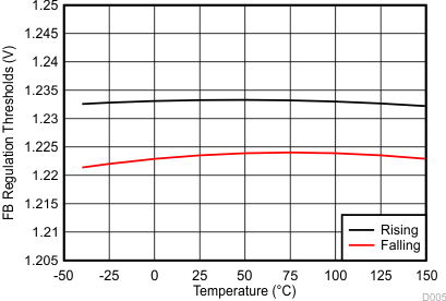
Figure 6-10 Feedback Comparator Voltage vs Temperature
GUID-64B5C355-7B2D-43D0-8782-45889A633CA2-low.gif
LM5165Y
Figure 6-12 VOUT Regulation Thresholds vs Temperature
GUID-275DE7E6-218C-4AC1-93AB-58B2415D4877-low.gif
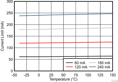
Figure 6-14 Peak Current Limits vs Temperature
GUID-1D92FAA9-73E3-4E22-A544-DD4349E3EE34-low.gif
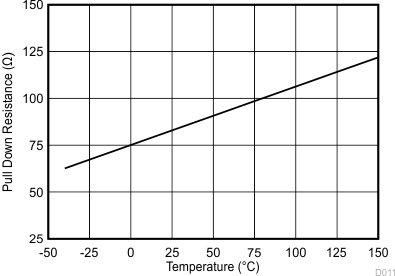
Figure 6-16 PGOOD and HYS Pulldown RDS(on) vs Temperature
GUID-608F3F2C-FFE2-40D5-8CA1-72DC223691D1-low.gif
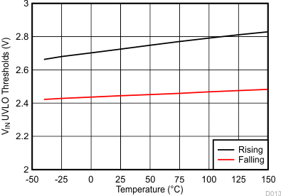
Figure 6-18 Internal VIN UVLO Voltage vs Temperature
GUID-1AD0860D-D088-477E-BE4E-1A7533DC97E0-low.gif
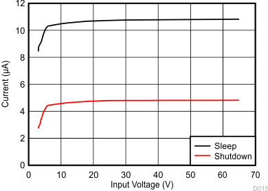
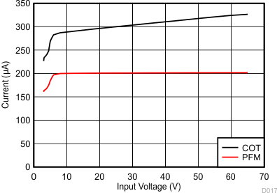
Figure 6-20 VIN Sleep and Shutdown Supply Current vs Input Voltage
GUID-ADC6A0AD-059B-4914-92FD-EAE006C3E442-low.gif
RRT = 75 kΩ
Figure 6-22 VIN Active Mode Supply Current vs Input Voltage
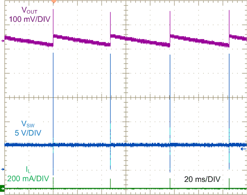
GUID-47D71A77-4CCB-4219-A25E-E28B28F8F71C-low.gifFigure 6-24 No Load Switching Waveforms, COT
GUID-60165EED-72F8-47CC-A7F8-BF516F4788DB-low.gifFigure 6-26 Short Circuit, COT
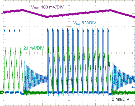
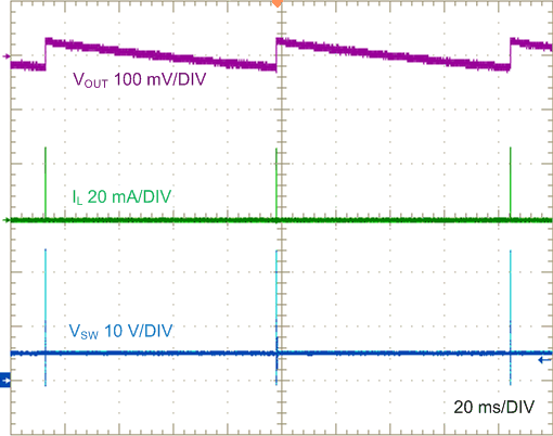
GUID-73BC04F4-103B-4EFB-81A0-EEE36872E74E-low.gifFigure 6-28 No Load Switching Waveforms, PFM
GUID-BB6D8FE4-1B93-4635-BD2A-4E4BF4576757-low.gifFigure 6-30 Short Circuit, PFM