JAJSCO0D November 2016 – August 2021 LM5170-Q1
PRODUCTION DATA
- 1 特長
- 2 アプリケーション
- 3 概要
- 4 Revision History
- 5 概要 (続き)
- 6 Pin Configuration and Functions
- 7 Specifications
-
8 Detailed Description
- 8.1 Overview
- 8.2 Functional Block Diagram
- 8.3
Feature Description
- 8.3.1 Bias Supply (VCC, VCCA)
- 8.3.2 Undervoltage Lockout (UVLO) and Master Enable or Disable
- 8.3.3 High Voltage Input (VIN, VINX)
- 8.3.4 Current Sense Amplifier
- 8.3.5 Control Commands
- 8.3.6 Channel Current Monitor (IOUT1, IOUT2)
- 8.3.7 Cycle-by-Cycle Peak Current Limit (IPK)
- 8.3.8 Error Amplifier
- 8.3.9 Ramp Generator
- 8.3.10 Soft Start
- 8.3.11 Gate Drive Outputs, Dead Time Programming and Adaptive Dead Time (HO1, HO2, LO1, LO2, DT)
- 8.3.12 PWM Comparator
- 8.3.13 Oscillator (OSC)
- 8.3.14 Synchronization to an External Clock (SYNCIN, SYNCOUT)
- 8.3.15 Diode Emulation
- 8.3.16 Power MOSFET Failure Detection and Failure Protection (nFAULT, BRKG, BRKS)
- 8.3.17 Overvoltage Protection (OVPA, OVPB)
- 8.4 Device Functional Modes
- 8.5 Programming
-
9 Application and Implementation
- 9.1 Application Information
- 9.2
Typical Application
- 9.2.1
60-A, Dual-Phase, 48-V to 12-V Bidirectional Converter
- 9.2.1.1 Design Requirements
- 9.2.1.2
Detailed Design Procedure
- 9.2.1.2.1 Determining the Duty Cycle
- 9.2.1.2.2 Oscillator Programming
- 9.2.1.2.3 Power Inductor, RMS and Peak Currents
- 9.2.1.2.4 Current Sense (RCS)
- 9.2.1.2.5 Current Setting Limits (ISETA or ISETD)
- 9.2.1.2.6 Peak Current Limit
- 9.2.1.2.7 Power MOSFETS
- 9.2.1.2.8 Bias Supply
- 9.2.1.2.9 Boot Strap
- 9.2.1.2.10 RAMP Generators
- 9.2.1.2.11 OVP
- 9.2.1.2.12 Dead Time
- 9.2.1.2.13 IOUT Monitors
- 9.2.1.2.14 UVLO Pin Usage
- 9.2.1.2.15 VIN Pin Configuration
- 9.2.1.2.16 Loop Compensation
- 9.2.1.2.17 Soft Start
- 9.2.1.2.18 ISET Pins
- 9.2.1.3 Application Curves
- 9.2.1
60-A, Dual-Phase, 48-V to 12-V Bidirectional Converter
- 10Power Supply Recommendations
- 11Layout
- 12Device and Documentation Support
- 13Mechanical, Packaging, and Orderable Information
パッケージ・オプション
メカニカル・データ(パッケージ|ピン)
- PHP|48
サーマルパッド・メカニカル・データ
- PHP|48
発注情報
8.3.5.3 Channel Current Setting Commands (ISETA or ISETD)
The LM5170-Q1 accepts the current setting command in the form of either an analog voltage or a PWM signal. The analog voltage uses the ISETA pin, and the PWM signal uses the ISETD pin. There is an internal ISETD decoder that converts the PWM duty ratio at the ISETD pin to an analog voltage at the ISETA pin. Owing to possible ground noise impact, TI recommends users to remove EN1 signal to achieve no load (0 A).
Figure 8-3 and Figure 8-4 show the pin configurations for current programming with an analog voltage or a PWM signal. The channel DC current is expressed in terms of resulted differential current sense voltage VCS_dc. When ISETA is used, the ISETD pin can be left open or connected to AGND. When ISETD is used, place a ceramic capacitor CISETA between the ISETA pin and AGND. CISETA and the internal 100-kΩ at the output of the ISETD decoder forms a low-pass RC filter to attenuate the ripple voltage on ISETA. However, the RC filter delays the ISETD dynamic change to be reflected on ISETA. To limit the delay not to exceed Tdelay_ISETD, the time constant of the RC filter should satisfy Equation 1.
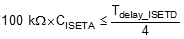
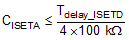
Therefore, the maximum CISETA should be determined by Equation 2:
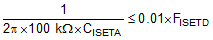
On the other hand, the time constant of the RC filter should be big enough for effective filtering. To attenuate the ripple by 40 dB, the RC filter corner frequency should be at least two decade below FISETD, that is, Equation 3
Therefore the minimum ISETD signal frequency should be determined by Equation 4:
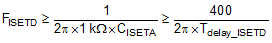
For instance, if ISETA is required to settle down to the steady-state in 1 ms following an ISETD duty ratio step change, namely Tdelay_ISETD < 1 ms, the user should select CISETA < 2.5 nF, and FISETD > 64 kHz. If Tdelay_ISETD < 0.1 ms, then CISETA < 250 pF, and FISETD> 640 kHz. Note that the feedback loop property causes additional delay for the actual current to settle to the new regulation level.
 Figure 8-3 Pin Configurations for Current Setting Using an Analog Voltage Signal
 Figure 8-4 Pin Configurations for Current Setting Using a PWM Signal
The ISETA pin is directly connected to the noninverting input of the error amplifier. By ISETA programming, the channel DC current is determined by Equation 5:

Or by Equation 6:
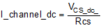
Or by Equation 7:
where
- Rcs is the channel current sensing resistor value.
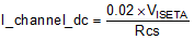
When using ISETD, the produced VISETA by the internal decoder is equal to the product of the effective duty ratio of the ISETD PWM signal (DISETD) and the 3.125-V internal reference voltage. The channel current is determined by Equation 8:

Or by Equation 9:

Or by Equation 10: