JAJSCO0D November 2016 – August 2021 LM5170-Q1
PRODUCTION DATA
- 1 特長
- 2 アプリケーション
- 3 概要
- 4 Revision History
- 5 概要 (続き)
- 6 Pin Configuration and Functions
- 7 Specifications
-
8 Detailed Description
- 8.1 Overview
- 8.2 Functional Block Diagram
- 8.3
Feature Description
- 8.3.1 Bias Supply (VCC, VCCA)
- 8.3.2 Undervoltage Lockout (UVLO) and Master Enable or Disable
- 8.3.3 High Voltage Input (VIN, VINX)
- 8.3.4 Current Sense Amplifier
- 8.3.5 Control Commands
- 8.3.6 Channel Current Monitor (IOUT1, IOUT2)
- 8.3.7 Cycle-by-Cycle Peak Current Limit (IPK)
- 8.3.8 Error Amplifier
- 8.3.9 Ramp Generator
- 8.3.10 Soft Start
- 8.3.11 Gate Drive Outputs, Dead Time Programming and Adaptive Dead Time (HO1, HO2, LO1, LO2, DT)
- 8.3.12 PWM Comparator
- 8.3.13 Oscillator (OSC)
- 8.3.14 Synchronization to an External Clock (SYNCIN, SYNCOUT)
- 8.3.15 Diode Emulation
- 8.3.16 Power MOSFET Failure Detection and Failure Protection (nFAULT, BRKG, BRKS)
- 8.3.17 Overvoltage Protection (OVPA, OVPB)
- 8.4 Device Functional Modes
- 8.5 Programming
-
9 Application and Implementation
- 9.1 Application Information
- 9.2
Typical Application
- 9.2.1
60-A, Dual-Phase, 48-V to 12-V Bidirectional Converter
- 9.2.1.1 Design Requirements
- 9.2.1.2
Detailed Design Procedure
- 9.2.1.2.1 Determining the Duty Cycle
- 9.2.1.2.2 Oscillator Programming
- 9.2.1.2.3 Power Inductor, RMS and Peak Currents
- 9.2.1.2.4 Current Sense (RCS)
- 9.2.1.2.5 Current Setting Limits (ISETA or ISETD)
- 9.2.1.2.6 Peak Current Limit
- 9.2.1.2.7 Power MOSFETS
- 9.2.1.2.8 Bias Supply
- 9.2.1.2.9 Boot Strap
- 9.2.1.2.10 RAMP Generators
- 9.2.1.2.11 OVP
- 9.2.1.2.12 Dead Time
- 9.2.1.2.13 IOUT Monitors
- 9.2.1.2.14 UVLO Pin Usage
- 9.2.1.2.15 VIN Pin Configuration
- 9.2.1.2.16 Loop Compensation
- 9.2.1.2.17 Soft Start
- 9.2.1.2.18 ISET Pins
- 9.2.1.3 Application Curves
- 9.2.1
60-A, Dual-Phase, 48-V to 12-V Bidirectional Converter
- 10Power Supply Recommendations
- 11Layout
- 12Device and Documentation Support
- 13Mechanical, Packaging, and Orderable Information
パッケージ・オプション
メカニカル・データ(パッケージ|ピン)
- PHP|48
サーマルパッド・メカニカル・データ
- PHP|48
発注情報
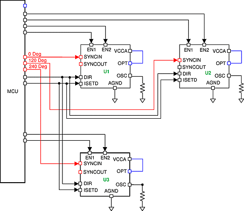
8.4.1.1 Multiphase in Star Configuration
Each LM5170 synchronizes to an external clock, and the clock signals should have appropriate phase delays among them for proper multiphase interleaving operation. The interleave angle between the two phases of each LM5170-Q1 can be programmed to 180° or 240° by the OPT pin.Table 8-1 summarizes the settings of the external clocks and the OPT pin state for multiphase configurations.
Table 8-1 Multiphase Configurations With Individual External Clock
| NUMBER OF PHASES | PHASE SHIFT BETWEEN EXTERNAL CLOCKS FOR MULTIPHASE INTERLEAVING | OPT LOGIC STATE(1) | CH-2 PHASE LAGGING VS CH-1 | NUMBER OF LM5170-Q1 CONTROLLERS NEEDED | NUMBER OF EXTERNAL CLOCKS NEEDED |
|---|---|---|---|---|---|
| 2 | 180° | 1 | 180° | 1 | 1 or 0 |
| 3 | 120° | 0 | 240° | 2 | 2 |
| 4 | 90° | 1 | 180° | 2 | 2 |
| 6 | 60° or 120° | 1 | 180° | 3 | 3 |
| 8 | 45° | 1 | 180° | 4 | 4 |
| 2xN | (180° / N) | 1 | 180° | N | N |
(1) OPT State = 0 when the pin connects to AGND, and 1 when the pin voltage is > 2.5 V.
 Figure 8-20 Example of Six Phase Star Configuration