JAJSM35B December 2015 – July 2021 LM53625-Q1 , LM53635-Q1
PRODUCTION DATA
- 1 特長
- 2 アプリケーション
- 3 概要
- 4 Revision History
- 5 Device Comparison
- 6 Pin Configuration and Functions
- 7 Specifications
- 8 Detailed Description
-
9 Application and Implementation
- 9.1 Application Information
- 9.2
Typical Applications
- 9.2.1 General Application
- 9.2.2 Fixed 5-V Output for USB-Type Applications
- 9.2.3 Fixed 3.3-V Output
- 9.2.4 Adjustable Output
- 9.3 What to Do and What Not to Do
- 10Power Supply Recommendations
- 11Layout
- 12Device and Documentation Support
- 13Mechanical, Packaging, and Orderable Information
パッケージ・オプション
デバイスごとのパッケージ図は、PDF版データシートをご参照ください。
メカニカル・データ(パッケージ|ピン)
- RNL|22
サーマルパッド・メカニカル・データ
- RNL|22
発注情報
6 Pin Configuration and Functions
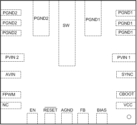
 Figure 6-1 RNL Package22-Pin VQFNTop View
Table 6-1 Pin Functions
| PIN | I/O(1) | DESCRIPTION | |
|---|---|---|---|
| NO. | NAME | ||
| 1 | VCC | A | Internal 3.1-V LDO output. Used as supply to internal control circuits. Connect a high-quality 4.7-µF capacitor from this pin to AGND. |
| 2 | CBOOT | P | Bootstrap capacitor connection for gate drivers. Connect a high quality 470-nF capacitor from this pin to the SW pin. |
| 3 | SYNC | I | Synchronization input to regulator. Used to synchronize the device switching frequency to a system clock. Triggers on rising edge of external clock; frequency must be in the range of 1.9 MHz and 2.3 MHz. |
| 4 | PVIN1 | P | Input supply to regulator. Connect input bypass capacitors directly to this pin and PGND pins. Connect PVIN1 and PVIN2 pins directly together at PCB. |
| 5, 6, 7, 8 | PGND1 | G | Power ground to internal low side MOSFET. These pins must be tied together on the PCB. Connect PGND1 and PGND2 directly together at PCB. Connect to AGND and system ground. |
| 9 | SW | P | Regulator switch node. Connect to power inductor. |
| 10, 11, 12, 13 | PGND2 | G | Power ground to internal low side MOSFET. These pins must be tied together. Connect PGND1 and PGND2 directly together at PCB. Connect to AGND and system ground. |
| 14 | PVIN2 | P | Input supply to regulator. Connect input bypass capacitors directly to this pin and PGND pins. Connect PVIN1 and PVIN2 pins directly together at PCB. |
| 15 | AVIN | A | Analog VIN, Connect to PVIN1 and PVIN2 on PCB. |
| 16 | FPWM | I | Do not float. Mode control input of regulator. High = FPWM, low = Automatic light load mode. |
| 17 | NC | — | No internal connection |
| 18 | EN | I | Enable input to regulator. High = on, Low = off. Can be connected to VIN. Do not float. |
| 19 | RESET | O | Open drain reset output flag. Connect to suitable voltage supply through a current limiting resistor. High = regulator OK, Low = regulator fault. Goes low when EN = low. |
| 20 | AGND | G | Analog ground for regulator and system. All electrical parameters are measured with respect to this pin. Connect to PGND on PCB |
| 21 | FB | A | Feedback input to regulator. Connect to output voltage node for fixed VOUT options. Connect to feedback voltage divider for adjustable option. |
| 22 | BIAS | P | Input to auxiliary bias regulator. Connect to output voltage node. |
(1) A = Analog, O = Output, I = Input, G = Ground, P = Power