JAJSKE1 October   2021 LM61430-Q1

PRODUCTION DATA  

  1. 特長
  2. アプリケーション
  3. 概要
  4. Revision History
  5. Device Comparison Table
  6. Pin Configuration and Functions
  7. Specifications
    1. 7.1 Absolute Maximum Ratings
    2. 7.2 ESD Ratings
    3. 7.3 Recommended Operating Conditions
    4. 7.4 Thermal Information
    5. 7.5 Electrical Characteristics
    6. 7.6 Timing Characteristics
    7. 7.7 Systems Characteristics
    8. 7.8 Typical Characteristics
  8. Detailed Description
    1. 8.1 Overview
    2. 8.2 Functional Block Diagram
    3. 8.3 Feature Description
      1. 8.3.1  EN/SYNC Uses for Enable and VIN UVLO
      2. 8.3.2  EN/SYNC Pin Uses for Synchronization
      3. 8.3.3  Clock Locking
      4. 8.3.4  Adjustable Switching Frequency
      5. 8.3.5  PGOOD Output Operation
      6. 8.3.6  Internal LDO, VCC UVLO, and BIAS Input
      7. 8.3.7  Bootstrap Voltage and VCBOOT-UVLO (CBOOT Pin)
      8. 8.3.8  Adjustable SW Node Slew Rate
      9. 8.3.9  Spread Spectrum
      10. 8.3.10 Soft Start and Recovery From Dropout
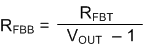
      11. 8.3.11 Output Voltage Setting
      12. 8.3.12 Overcurrent and Short Circuit Protection
      13. 8.3.13 Thermal Shutdown
      14. 8.3.14 Input Supply Current
    4. 8.4 Device Functional Modes
      1. 8.4.1 Shutdown Mode
      2. 8.4.2 Standby Mode
      3. 8.4.3 Active Mode
        1. 8.4.3.1 Auto Mode - Light-Load Operation
          1. 8.4.3.1.1 Diode Emulation
          2. 8.4.3.1.2 Frequency Reduction
        2. 8.4.3.2 FPWM Mode - Light-Load Operation
          1. 8.4.3.2.1 CCM Mode
        3. 8.4.3.3 Minimum On Time (High Input Voltage) Operation
        4. 8.4.3.4 Dropout
  9. Application and Implementation
    1. 9.1 Application Information
    2. 9.2 Typical Application
      1. 9.2.1 Design Requirements
      2. 9.2.2 Detailed Design Procedure
        1. 9.2.2.1  Choosing the Switching Frequency
        2. 9.2.2.2  Setting the Output Voltage
        3. 9.2.2.3  Inductor Selection
        4. 9.2.2.4  Output Capacitor Selection
        5. 9.2.2.5  Input Capacitor Selection
        6. 9.2.2.6  BOOT Capacitor
        7. 9.2.2.7  BOOT Resistor
        8. 9.2.2.8  VCC
        9. 9.2.2.9  BIAS
        10. 9.2.2.10 CFF and RFF Selection
        11. 9.2.2.11 External UVLO
      3. 9.2.3 Application Curves
  10. 10Power Supply Recommendations
  11. 11Layout
    1. 11.1 Layout Guidelines
      1. 11.1.1 Ground and Thermal Considerations
    2. 11.2 Layout Example
  12. 12Device and Documentation Support
    1. 12.1 Device Support
      1. 12.1.1 Third-Party Products Disclaimer
    2. 12.2 Documentation Support
      1. 12.2.1 Related Documentation
    3. 12.3 Receiving Notification of Documentation Updates
    4. 12.4 サポート・リソース
    5. 12.5 Trademarks
    6. 12.6 Electrostatic Discharge Caution
    7. 12.7 Glossary
  13. 13Mechanical, Packaging, and Orderable Information

パッケージ・オプション

メカニカル・データ(パッケージ|ピン)
サーマルパッド・メカニカル・データ
発注情報

Output Voltage Setting

A feedback resistor divider network between the output voltage and the FB pin is used to set output voltage level. See Figure 8-10.

GUID-FDB9FC11-2B95-4F16-8D5E-6029B8CA1BE6-low.gifFigure 8-10 Setting Output Voltage of Adjustable Versions

The LM61430-Q1 uses a 1-V reference voltage for the feedback (FB) pin. The FB pin voltage is regulated by the internal controller to be the same as the reference voltage. The output voltage level is then set by the ratio of the resistor divider. Equation 3 can be used to determine RFBB for a desired output voltage and a given RFBT. Usually RFBT is between 10 kΩ and 1 MΩ. 100 kΩ is recommended for RFBT for improved noise immunity compared to 1 MΩ and reduced current consumption compared to lower resistance values.

Equation 3. GUID-AEE23453-7760-4946-A5E9-540942C1C7DA-low.gif

In addition, a feedforward capacitor, CFF, connected in parallel with RFBT can be required to optimize the transient response.