JAJSE52B November 2017 – May 2021 LM73605-Q1 , LM73606-Q1
PRODUCTION DATA
- 1 特長
- 2 アプリケーション
- 3 概要
- 4 Revision History
- 5 Device Comparison
- 6 Pin Configuration and Functions
- 7 Specifications
-
8 Detailed Description
- 8.1 Overview
- 8.2 Functional Block Diagram
- 8.3
Feature Description
- 8.3.1 Synchronous Step-Down Regulator
- 8.3.2 Auto Mode and FPWM Mode
- 8.3.3 Fixed-Frequency Peak Current-Mode Control
- 8.3.4 Adjustable Output Voltage
- 8.3.5 Enable and UVLO
- 8.3.6 Internal LDO, VCC_UVLO, and BIAS Input
- 8.3.7 Soft Start and Voltage Tracking
- 8.3.8 Adjustable Switching Frequency
- 8.3.9 Frequency Synchronization and Mode Setting
- 8.3.10 Internal Compensation and CFF
- 8.3.11 Bootstrap Capacitor and VBOOT-UVLO
- 8.3.12 Power-Good and Overvoltage Protection
- 8.3.13 Overcurrent and Short-Circuit Protection
- 8.3.14 Thermal Shutdown
- 8.4 Device Functional Modes
- 9 Layout
- 10Device and Documentation Support
パッケージ・オプション
メカニカル・データ(パッケージ|ピン)
- RNP|30
サーマルパッド・メカニカル・データ
- RNP|30
発注情報
8.3.7 Soft Start and Voltage Tracking
The LM73605-Q1/6-Q1 controlled output voltage ramp during start-up. The soft-start feature reduces inrush current during start-up and improves system performance and reliability.
If the SS/TRK pin is floating, the LM73605-Q1/6-Q1 up following the fixed internal soft-start ramp.
If longer soft-start time is desired, an external capacitor can be added from SS/TRK pin to ground. There is a 2-µA (typical) internal current source, ISSC, to charge the external capacitor. For a desired soft-start time tSS, capacitance of CSS can be found by Equation 12.
where
- CSS = soft-start capacitor value (F)
- ISSC = soft-start charging current (A)
- tSS = desired soft-start time or times
The FB voltage always follows the lower potential of the internal voltage ramp or the voltage on the SS/TRK pin. Thus, the soft-start time can only be extended longer than the internal soft-start time by connecting CSS. Use CSS to extend soft-start time when there are a large amount of output capacitors, the output voltage is high, or the output is heavily loaded during start-up.
LM73605-Q1/6-Q1 operating in diode emulation mode during start-up regardless of mode setting. The device is capable of starting up into pre-biased output conditions. During start-up, the device sets the minimum inductor current to zero to avoid back charging the input capacitors.
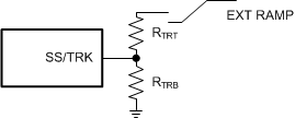
LM73605-Q1/6-Q1 can track an external voltage ramp applied to the SS/TRK pin, if the ramp is slower than the internal soft-start ramp. The external ramp final voltage after start-up must be greater than 1.5 V to avoid noise interfering with the reference voltage. Figure 8-9 shows how to use resistor divider to set VOUT to follow an external ramp.
 Figure 8-9 Soft-start Tracking External Ramp
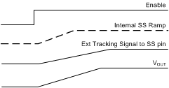
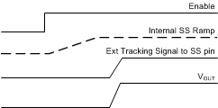
VOUT tracking also provides the option of ramping up faster than the internal start-up ramp. The FB voltage always follows the lower potential of the internal voltage ramp and the voltage on the SS/TRK pin. Figure 8-10 shows the case when VOUT ramps slower than the internal ramp, while Figure 8-11 shows when VOUT ramps faster than the internal ramp. If the tracking ramp is delayed after the internal ramp is completed, VFB follows the tracking ramp even if it is faster than the internal ramp. Faster start-up time may result in large inductor current during start-up. Use with special care.
 Figure 8-10 Tracking With Longer Start-up Time Than the Internal Ramp
 Figure 8-11 Tracking With Shorter Start-up Time Than the Internal Ramp
The SS/TRK pin is discharged to ground by an internal pulldown resistor RSSD when the output voltage is shutting down, such as in the event of UVLO, thermal shutdown, hiccup, or VEN = 0. If a large CSS is used, and the time when VEN = 0 V is very short, the CSS may not be fully discharged before the next soft start. Under this condition, the FB voltage follows the internal ramp slew rate until the voltage on CSS is reached, then follow the slew rate defined by CSS.