JAJSE52B November 2017 – May 2021 LM73605-Q1 , LM73606-Q1
PRODUCTION DATA
- 1 特長
- 2 アプリケーション
- 3 概要
- 4 Revision History
- 5 Device Comparison
- 6 Pin Configuration and Functions
- 7 Specifications
-
8 Detailed Description
- 8.1 Overview
- 8.2 Functional Block Diagram
- 8.3
Feature Description
- 8.3.1 Synchronous Step-Down Regulator
- 8.3.2 Auto Mode and FPWM Mode
- 8.3.3 Fixed-Frequency Peak Current-Mode Control
- 8.3.4 Adjustable Output Voltage
- 8.3.5 Enable and UVLO
- 8.3.6 Internal LDO, VCC_UVLO, and BIAS Input
- 8.3.7 Soft Start and Voltage Tracking
- 8.3.8 Adjustable Switching Frequency
- 8.3.9 Frequency Synchronization and Mode Setting
- 8.3.10 Internal Compensation and CFF
- 8.3.11 Bootstrap Capacitor and VBOOT-UVLO
- 8.3.12 Power-Good and Overvoltage Protection
- 8.3.13 Overcurrent and Short-Circuit Protection
- 8.3.14 Thermal Shutdown
- 8.4 Device Functional Modes
- 9 Layout
- 10Device and Documentation Support
パッケージ・オプション
メカニカル・データ(パッケージ|ピン)
- RNP|30
サーマルパッド・メカニカル・データ
- RNP|30
発注情報
9.1.1 Layout For EMI Reduction
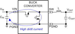
To optimize EMI performance, place the components in the high di/dt current path, as shown in Figure 9-1, as close as possible to each other. When the components are close to each other, the area of the loop enclosed by these components, and the parasitic inductance of this loop, are minimized. The noises generated by the pulsing current and parasitic inductances are then minimized.
 Figure 9-1 Pulsing Current Path of Buck Converter
In a buck converter, the high di/dt current path is composed of the HS and LS MOSFETs and the input capacitors. Because the two MOSFETs are integrated inside the device, they are closer to each other than in discrete solutions. PVIN and PGND pins are the connections from the MOSFETs to the input capacitors. The first step of the layout must be placing the input capacitors, especially the small value ceramic bypass one, as close as possible to PVIN and PGND pins.
The LM73605-Q1/6-Q1 pinout is optimized for low EMI layout. Multiple pins are used for PVIN and PGND to minimized bond wire resistances and inductances. The PVIN and PGND pins are right next to each other to simplify optimal layout. The CBOOT pin is placed next to SW pin for easy and compact CBOOT capacitor layout.