JAJSM66A June 2021 – December 2021 LM74701-Q1
PRODUCTION DATA
- 1 特長
- 2 アプリケーション
- 3 概要
- 4 Revision History
- 5 Pin Configuration and Functions
- 6 Specifications
- 7 Parameter Measurement Information
- 8 Detailed Description
- 9 Application and Implementation
- 10Power Supply Recommendations
- 11Layout
- 12Device and Documentation Support
- 13Mechanical, Packaging, and Orderable Information
パッケージ・オプション
デバイスごとのパッケージ図は、PDF版データシートをご参照ください。
メカニカル・データ(パッケージ|ピン)
- DDF|8
サーマルパッド・メカニカル・データ
発注情報
8.4.2.3 VDS Clamp Mode
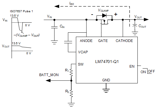
The LM74701-Q1 features an integrated VDS clamp that operates the external MOSFET as an active clamp element to dissipate transient energy of automotive EMC transients such as ISO7637-2 pulse 1 where there is no output voltage hold up requirement and system is allowed to turn off during such EMC transients. VDS clamp threshold is selected such that LM74701-Q1 does not engage into VDS clamp operation thereby ensuring the FET remains OFF during the RCB state for the system level EMC tests where output voltage hold up is required such as input short interruptions and micro cuts (LV124 E-10, ISO16750-2).
When the ISO7637 pulse 1 is applied at the input of LM74701-Q1:
- After the voltage drop across ANODE to CATHODE reaches V(AK_REV) threshold, the device GATE goes low and turns OFF the MOSFET.
- After the voltage across the drain and source of the MOSFET reaches VCLAMP level (34-V minimum), GATE is turned ON back in the saturation region, operating external MOSFET as an active clamp and dissipates the ISO7637 pulse 1 energy. The typical circuit operation of LM74701-Q1 during ISO7637 pulse 1 is shown in Figure 8-4.
 Figure 8-4 LM74701-Q1 Operation During VDS Clamp Mode
Note that the reverse current flows from VOUT back to input during the ISO7637 pulse 1 transient event, thus discharging VOUT capacitor. LM74701-Q1 CATHODE pin can handle negative voltage, however, if loads connected to the output of LM74701-Q1 can not handle negative voltage then the output hold up capacitor must be selected to ensure that VOUT does not go negative during ISO7637 pulse 1 test. For all the other ISO7637 pulses (that is, pulse 2a, 2b, 3a, 3b), which are short duration transient events, the input and output capacitors filtering effect suppresses these pulses.
For additional details on system level EMC performance of LM74701-Q1, refer to Application Information.