JAJSK05D September   2020  – March 2022 LMG3422R030 , LMG3425R030

PRODUCTION DATA  

  1. 特長
  2. アプリケーション
  3. 概要
  4. Revision History
  5. Device Comparison
  6. Pin Configuration and Functions
  7. Specifications
    1. 7.1 Absolute Maximum Ratings
    2. 7.2 ESD Ratings
    3. 7.3 Recommended Operating Conditions
    4. 7.4 Thermal Information
    5. 7.5 Electrical Characteristics
    6. 7.6 Switching Characteristics
    7. 7.7 Typical Characteristics
  8. Parameter Measurement Information
    1. 8.1 Switching Parameters
      1. 8.1.1 Turn-On Times
      2. 8.1.2 Turn-Off Times
      3. 8.1.3 Drain-Source Turn-On Slew Rate
      4. 8.1.4 Turn-On and Turn-Off Switching Energy
  9. Detailed Description
    1. 9.1 Overview
    2. 9.2 Functional Block Diagram
    3. 9.3 Feature Description
      1. 9.3.1  GaN FET Operation Definitions
      2. 9.3.2  Direct-Drive GaN Architecture
      3. 9.3.3  Drain-Source Voltage Capability
      4. 9.3.4  Internal Buck-Boost DC-DC Converter
      5. 9.3.5  VDD Bias Supply
      6. 9.3.6  Auxiliary LDO
      7. 9.3.7  Fault Detection
        1. 9.3.7.1 Overcurrent Protection and Short-Circuit Protection
        2. 9.3.7.2 Overtemperature Shutdown
        3. 9.3.7.3 UVLO Protection
        4. 9.3.7.4 Fault Reporting
      8. 9.3.8  Drive Strength Adjustment
      9. 9.3.9  Temperature-Sensing Output
      10. 9.3.10 Ideal-Diode Mode Operation
    4. 9.4 Device Functional Modes
  10. 10Application and Implementation
    1. 10.1 Application Information
    2. 10.2 Typical Application
      1. 10.2.1 Design Requirements
      2. 10.2.2 Detailed Design Procedure
        1. 10.2.2.1 Slew Rate Selection
          1. 10.2.2.1.1 Start-Up and Slew Rate With Bootstrap High-Side Supply
        2. 10.2.2.2 Signal Level-Shifting
        3. 10.2.2.3 Buck-Boost Converter Design
      3. 10.2.3 Application Curves
    3. 10.3 Do's and Don'ts
  11. 11Power Supply Recommendations
    1. 11.1 Using an Isolated Power Supply
    2. 11.2 Using a Bootstrap Diode
      1. 11.2.1 Diode Selection
      2. 11.2.2 Managing the Bootstrap Voltage
  12. 12Layout
    1. 12.1 Layout Guidelines
      1. 12.1.1 Solder-Joint Reliability
      2. 12.1.2 Power-Loop Inductance
      3. 12.1.3 Signal-Ground Connection
      4. 12.1.4 Bypass Capacitors
      5. 12.1.5 Switch-Node Capacitance
      6. 12.1.6 Signal Integrity
      7. 12.1.7 High-Voltage Spacing
      8. 12.1.8 Thermal Recommendations
    2. 12.2 Layout Examples
  13. 13Device and Documentation Support
    1. 13.1 Documentation Support
      1. 13.1.1 Related Documentation
    2. 13.2 Receiving Notification of Documentation Updates
    3. 13.3 サポート・リソース
    4. 13.4 Trademarks
    5. 13.5 Electrostatic Discharge Caution
    6. 13.6 Export Control Notice
    7. 13.7 Glossary
  14. 14Mechanical, Packaging, and Orderable Information

パッケージ・オプション

デバイスごとのパッケージ図は、PDF版データシートをご参照ください。

メカニカル・データ(パッケージ|ピン)
  • RQZ|54
サーマルパッド・メカニカル・データ
発注情報

Typical Application

CAUTION: For applications where the drain slew rate is programmed for greater than a typical 100 V/ns (RRDRV < 10 kΩ or VRDRV = 5 V), the following application design modifications must be implemented to minimize the risk of LDO5V pin damage.
  1. Remove C2.
  2. Put a 10-Ω resistor between the U1 LDO5V pin and C10. No other components must be between the resistor and the U1 LDO5V pin.
  3. Remove C12.
  4. Put a 10-Ω resistor between the U2 LDO5V pin and C27. No other components must be between the resistor and the U2 LDO5V pin.
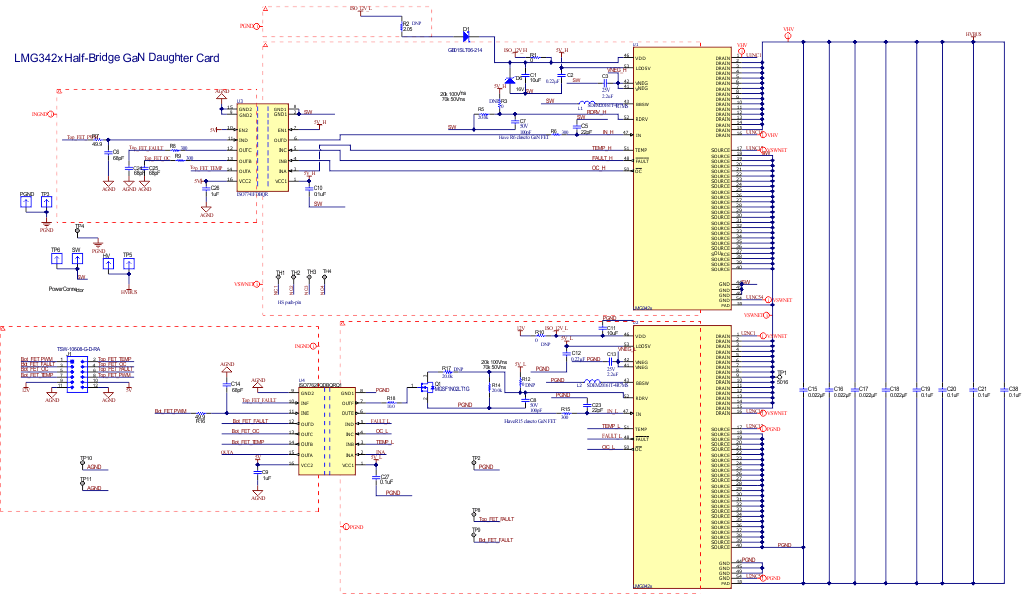
GUID-20211130-SS0I-6R2J-H3K4-CSDFB3FBF7SJ-low.gif Figure 10-1 Typical Half-Bridge Application