JAJSK05D September 2020 – March 2022 LMG3422R030 , LMG3425R030
PRODUCTION DATA
- 1 特長
- 2 アプリケーション
- 3 概要
- 4 Revision History
- 5 Device Comparison
- 6 Pin Configuration and Functions
- 7 Specifications
- 8 Parameter Measurement Information
-
9 Detailed Description
- 9.1 Overview
- 9.2 Functional Block Diagram
- 9.3
Feature Description
- 9.3.1 GaN FET Operation Definitions
- 9.3.2 Direct-Drive GaN Architecture
- 9.3.3 Drain-Source Voltage Capability
- 9.3.4 Internal Buck-Boost DC-DC Converter
- 9.3.5 VDD Bias Supply
- 9.3.6 Auxiliary LDO
- 9.3.7 Fault Detection
- 9.3.8 Drive Strength Adjustment
- 9.3.9 Temperature-Sensing Output
- 9.3.10 Ideal-Diode Mode Operation
- 9.4 Device Functional Modes
- 10Application and Implementation
- 11Power Supply Recommendations
- 12Layout
- 13Device and Documentation Support
- 14Mechanical, Packaging, and Orderable Information
パッケージ・オプション
デバイスごとのパッケージ図は、PDF版データシートをご参照ください。
メカニカル・データ(パッケージ|ピン)
- RQZ|54
サーマルパッド・メカニカル・データ
発注情報
10.2.2.3 Buck-Boost Converter Design
The buck-boost converter generates the negative voltage to turn off the direct-drive GaN device. While the buck-boost converter is controlled internally, it requires an external power inductor and output capacitor. The converter is designed to use a 4.7-µH inductor and a 2.2-µF output capacitor.
As the peak current of the buck-boost is subject to two different peak current limits which are 0.4 A and 1 A for low and high frequency operation (see Internal Buck-Boost DC-DC Converter), so the inductor must have a saturation current well above the rated peak current limit. After the higher limit is established by switching at a higher frequency, the current limit does not go back to the lower level even when GaN device is then switched at a lower frequency. Therefore, select an inductor according to the higher 1-A limit if higher frequency GaN operation is anticipated.
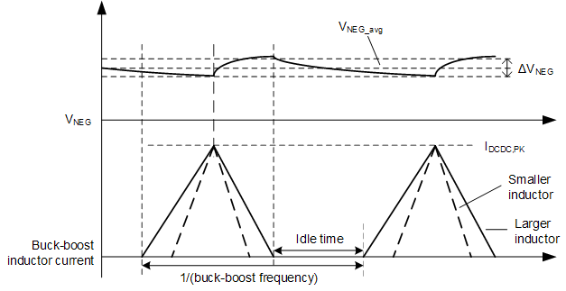
The buck-boost converter uses a peak current hysteretic control. As shown in Figure 10-2, the inductor current increases at the beginning of a switching cycle until the inductor reaches the peak current limit. The inductor current goes down to zero. The idle time between each current pulse is determined automatically by the output current, and can be reduced to zero. Therefore, the maximum output current happens when the idle time is zero, and is decided by the peak current but independent of the inductor value.
A minimum inductance value of 3 µH is preferred for the buck-boost converter so that the di/dt across the inductor is not too high. This leaves enough margin for the control loop to respond. As a result, the maximum di/dt of the inductor is limited to 6 A/µs. On the other hand, large inductance also limits the transient response for stable output voltage, and it is preferred to have inductors less than 10 µH.
 Figure 10-2 Buck-Boost Converter Inductor Current