JAJSF77A April 2018 – January 2022 LMK00334-Q1
PRODUCTION DATA
- 1 特長
- 2 アプリケーション
- 3 概要
- 4 Revision History
- 5 Pin Configuration and Functions
- 6 Specifications
- 7 Parameter Measurement Information
- 8 Detailed Description
- 9 Application and Implementation
- 10Power Supply Recommendations
- 11Layout
- 12Device and Documentation Support
- 13Mechanical, Packaging, and Orderable Information
9.2.1.2 Crystal Interface
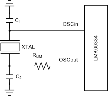
The LMK00334-Q1 has an integrated crystal oscillator circuit that supports a fundamental mode, AT-cut crystal. The crystal interface is shown in Figure 9-5.
 Figure 9-5 Crystal Interface
The load capacitance (CL) is specific to the crystal, but usually on the order of 18 to 20 pF. While CL is specified for the crystal, the OSCin input capacitance (CIN = 1 pF typical) of the device and PCB stray capacitance (CSTRAY is approximately around 1 to 3 pF) can affect the discrete load capacitor values, C1 and C2.
For the parallel resonant circuit, the discrete capacitor values can be calculated as follows:
Typically, C1 = C2 for optimum symmetry, so Equation 1 can be rewritten in terms of C1 only:
Finally, solve for C1:
Section 6.5 provides crystal interface specifications with conditions that ensure start-up of the crystal, but it does not specify crystal power dissipation. The designer must ensure the crystal power dissipation does not exceed the maximum drive level specified by the crystal manufacturer. Overdriving the crystal can cause premature aging, frequency shift, and eventual failure. Drive level should be held at a sufficient level necessary to start up and maintain steady-state operation.
The power dissipated in the crystal, PXTAL, can be computed by:
where
- IRMS is the RMS current through the crystal.
- RESR is the maximum equivalent series resistance specified for the crystal
- CL is the load capacitance specified for the crystal
- C0 is the minimum shunt capacitance specified for the crystal
IRMS can be measured using a current probe (Tektronix CT-6 or equivalent, for example) placed on the leg of the crystal connected to OSCout with the oscillation circuit active.
As shown in Figure 9-5, an external resistor, RLIM, can be used to limit the crystal drive level, if necessary. If the power dissipated in the selected crystal is higher than the drive level specified for the crystal with RLIM shorted, then a larger resistor value is mandatory to avoid overdriving the crystal. However, if the power dissipated in the crystal is less than the drive level with RLIM shorted, then a zero value for RLIM can be used. As a starting point, a suggested value for RLIM is 1.5 kΩ.