JAJSJN5B december 2020 – june 2023 LMK1D1204 , LMK1D1208
PRODUCTION DATA
- 1
- 1 特長
- 2 アプリケーション
- 3 概要
- 4 Revision History
- 5 Device Comparison
- 6 Pin Configuration and Functions
- 7 Specifications
- 8 Parameter Measurement Information
- 9 Detailed Description
- 10Application and Implementation
- 11Device and Documentation Support
- 12Mechanical, Packaging, and Orderable Information
パッケージ・オプション
メカニカル・データ(パッケージ|ピン)
- RGT|16
サーマルパッド・メカニカル・データ
- RGT|16
発注情報
6 Pin Configuration and Functions
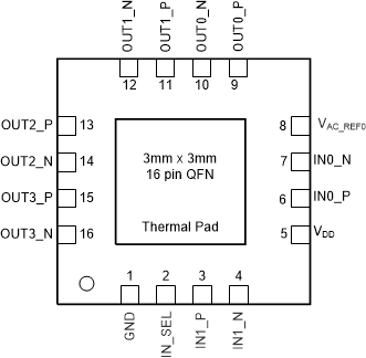
 Figure 6-1 LMK1D1204: RGT Package
16-Pin VQFN Top View
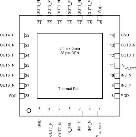
 Figure 6-2 LMK1D1208: RHD Package
28-Pin VQFN Top View
Figure 6-2 LMK1D1208: RHD Package
28-Pin VQFN Top ViewTable 6-1 Pin Functions
| PIN | TYPE(1) | DESCRIPTION | ||
|---|---|---|---|---|
| NAME | LMK1D1204 | LMK1D1208 | ||
| DIFFERENTIAL/SINGLE-ENDED CLOCK INPUT | ||||
| IN0_P | 6 | 9 | I | Primary: Differential input pair or single-ended input |
| IN0_N | 7 | 10 | ||
| IN1_P | 3 | 5 | I | Secondary: Differential input pair or single-ended input. |
| IN1_N | 4 | 6 | Note that INP0, INN0 are used indistinguishably with IN0_P, IN0_N. | |
| INPUT SELECT | ||||
| IN_SEL | 2 | 4 | I | Input Selection with an internal 500-kΩ pullup and 320-kΩ pulldown resistor, selects input port; (See Table 9-1) |
| BIAS VOLTAGE OUTPUT | ||||
| VAC_REF0 | 8 | 11 | O | Bias voltage output for capacitive coupled inputs. If used, TI recommends using a 0.1-µF capacitor to GND on this pin. |
| VAC_REF1 | — | 7 | ||
| DIFFERENTIAL CLOCK OUTPUT | ||||
| OUT0_P | 9 | 12 | O | Differential LVDS output pair number 0 |
| OUT0_N | 10 | 13 | ||
| OUT1_P | 11 | 16 | O | Differential LVDS output pair number 1 |
| OUT1_N | 12 | 17 | ||
| OUT2_P | 13 | 18 | O | Differential LVDS output pair number 2 |
| OUT2_N | 14 | 19 | ||
| OUT3_P | 15 | 20 | O | Differential LVDS output pair number 3 |
| OUT3_N | 16 | 21 | ||
| OUT4_P | — | 22 | O | Differential LVDS output pair number 4 |
| OUT4_N | 23 | |||
| OUT5_P | — | 24 | O | Differential LVDS output pair number 5 |
| OUT5_N | 25 | |||
| OUT6_P | — | 26 | O | Differential LVDS output pair number 6 |
| OUT6_N | 27 | |||
| OUT7_P | — | 2 | O | Differential LVDS output pair number 7 |
| OUT7_N | 3 | |||
| SUPPLY VOLTAGE | ||||
| VDD | 5 | 8 | P | Device Power Supply (1.8V or 2.5V or 3.3V) |
| 15 | ||||
| 28 | ||||
| GROUND | ||||
| GND | 1 | 1 | G | Ground |
| — | 14 | |||
| MISC | ||||
| DAP | DAP | DAP | GND | Die Attach Pad. Connect to the PCB ground plane for heat dissipation. |
| NC | — | — | NC | No Connection |
(1) G = Ground, I = Input, O = Output, P = Power