JAJSFN4C June 2018 – October 2020 LMR33620-Q1
PRODUCTION DATA
- 1 特長
- 2 アプリケーション
- 3 概要
- 4 改訂履歴
- 5 Pin Configuration and Functions
- 6 Specifications
- 7 Detailed Description
-
8 Application and Implementation
- 8.1 Application Information
- 8.2
Typical Application
- 8.2.1 Design Requirements
- 8.2.2
Detailed Design Procedure
- 8.2.2.1 Custom Design With WEBENCH® Tools
- 8.2.2.2 Choosing the Switching Frequency
- 8.2.2.3 Setting the Output Voltage
- 8.2.2.4 Inductor Selection
- 8.2.2.5 Output Capacitor Selection
- 8.2.2.6 Input Capacitor Selection
- 8.2.2.7 CBOOT
- 8.2.2.8 VCC
- 8.2.2.9 CFF Selection
- 8.2.2.10 External UVLO
- 8.2.2.11 Maximum Ambient Temperature
- 8.2.3 Application Curves
- 8.3 What to Do and What Not to Do
- 9 Power Supply Recommendations
- 10Layout
- 11Device and Documentation Support
パッケージ・オプション
デバイスごとのパッケージ図は、PDF版データシートをご参照ください。
メカニカル・データ(パッケージ|ピン)
- RNX|12
サーマルパッド・メカニカル・データ
- RNX|12
発注情報
9 Power Supply Recommendations
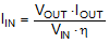
The characteristics of the input supply must be compatible with Section 6.1 and Section 6.3 found in this data sheet. In addition, the input supply must be capable of delivering the required input current to the loaded regulator. The average input current can be estimated with Equation 12, where η is the efficiency.
If the regulator is connected to the input supply through long wires or PCB traces, special care is required to achieve good performance. The parasitic inductance and resistance of the input cables can have an adverse effect on the operation of the regulator. The parasitic inductance, in combination with the low-ESR, ceramic input capacitors, can form an under damped resonant circuit, resulting in overvoltage transients at the input to the regulator. The parasitic resistance can cause the voltage at the VIN pin to dip whenever a load transient is applied to the output. If the application is operating close to the minimum input voltage, this dip can cause the regulator to momentarily shutdown and reset. The best way to solve these kind of issues is to reduce the distance from the input supply to the regulator and/or use an aluminum or tantalum input capacitor in parallel with the ceramics. The moderate ESR of these types of capacitors help damp the input resonant circuit and reduce any overshoots. A value in the range of 20 µF to 100 µF is usually sufficient to provide input damping and help to hold the input voltage steady during large load transients.
Sometimes, for other system considerations, an input filter is used in front of the regulator. This can lead to instability, as well as some of the effects mentioned above, unless it is designed carefully. The user guide AN-2162 Simple Success With Conducted EMI From DCDC Converters provides helpful suggestions when designing an input filter for any switching regulator.
In some cases, a transient voltage suppressor (TVS) is used on the input of regulators. One class of this device has a snap-back characteristic (thyristor type). The use of a device with this type of characteristic is not recommended. When the TVS fires, the clamping voltage falls to a very low value. If this voltage is less than the output voltage of the regulator, the output capacitors discharge through the device back to the input. This uncontrolled current flow can damage the device.
The input voltage must not be allowed to fall below the output voltage. In this scenario, such as a shorted input test, the output capacitors discharges through the internal parasitic diode found between the VIN and SW pins of the device. During this condition, the current can become uncontrolled, possibly causing damage to the device. If this scenario is considered likely, then a Schottky diode between the input supply and the output should be used.