JAJSFN4C June 2018 – October 2020 LMR33620-Q1
PRODUCTION DATA
- 1 特長
- 2 アプリケーション
- 3 概要
- 4 改訂履歴
- 5 Pin Configuration and Functions
- 6 Specifications
- 7 Detailed Description
-
8 Application and Implementation
- 8.1 Application Information
- 8.2
Typical Application
- 8.2.1 Design Requirements
- 8.2.2
Detailed Design Procedure
- 8.2.2.1 Custom Design With WEBENCH® Tools
- 8.2.2.2 Choosing the Switching Frequency
- 8.2.2.3 Setting the Output Voltage
- 8.2.2.4 Inductor Selection
- 8.2.2.5 Output Capacitor Selection
- 8.2.2.6 Input Capacitor Selection
- 8.2.2.7 CBOOT
- 8.2.2.8 VCC
- 8.2.2.9 CFF Selection
- 8.2.2.10 External UVLO
- 8.2.2.11 Maximum Ambient Temperature
- 8.2.3 Application Curves
- 8.3 What to Do and What Not to Do
- 9 Power Supply Recommendations
- 10Layout
- 11Device and Documentation Support
パッケージ・オプション
デバイスごとのパッケージ図は、PDF版データシートをご参照ください。
メカニカル・データ(パッケージ|ピン)
- RNX|12
サーマルパッド・メカニカル・データ
- RNX|12
発注情報
8.2.2.10 External UVLO
In some cases, an input UVLO level different than that provided internal to the device is needed. This can be accomplished by using the circuit shown in Figure 8-6. The input voltage at which the device turns on is designated VON while the turnoff voltage is VOFF. First, a value for RENB is chosen in the range of 10 kΩ to 100 kΩ and then Equation 10 is used to calculate RENT and VOFF.
 Figure 8-6 Setup for External UVLO Application
Equation 10. 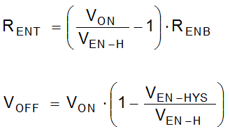
where
- VON = VIN turnon voltage
- VOFF = VIN turnoff voltage