JAJSFY3D August 2018 – August 2022 LMR36006-Q1
PRODUCTION DATA
- 1 特長
- 2 アプリケーション
- 3 概要
- 4 Revision History
- 5 Device Comparison Table
- 6 Pin Configuration and Functions
- 7 Specifications
- 8 Detailed Description
-
9 Application and Implementation
- 9.1 Application Information
- 9.2
Typical Application
- 9.2.1
Design 1: Low Power 24-V, 600-mA PFM Converter
- 9.2.1.1 Design Requirements
- 9.2.1.2
Detailed Design Procedure
- 9.2.1.2.1 Custom Design With WEBENCH Tools
- 9.2.1.2.2 Choosing the Switching Frequency
- 9.2.1.2.3 Setting the Output Voltage
- 9.2.1.2.4 Inductor Selection
- 9.2.1.2.5 Output Capacitor Selection
- 9.2.1.2.6 Input Capacitor Selection
- 9.2.1.2.7 CBOOT
- 9.2.1.2.8 VCC
- 9.2.1.2.9 CFF Selection
- 9.2.1.2.10 Maximum Ambient Temperature
- 9.2.1.3 Application Curves
- 9.2.2 Design 2: High Density 12-V , 600-mA FPWM Converter
- 9.2.1
Design 1: Low Power 24-V, 600-mA PFM Converter
- 9.3 What to Do and What Not to Do
- 10Power Supply Recommendations
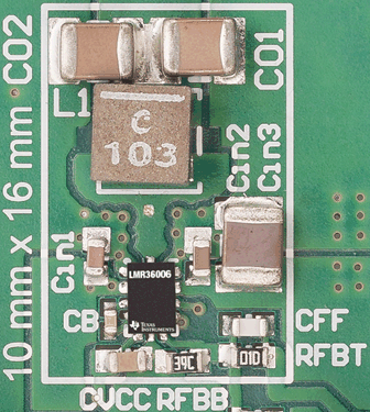
- 11Layout
- 12Device and Documentation Support
- 13Mechanical, Packaging, and Orderable Information
パッケージ・オプション
メカニカル・データ(パッケージ|ピン)
- RNX|12
サーマルパッド・メカニカル・データ
- RNX|12
発注情報
3 概要
LMR36006-Q1 レギュレータは使いやすい同期整流降圧 DC/DC コンバータです。ハイサイドとローサイドのパワー MOSFET を内蔵しており、4.2V~60V の広い入力電圧範囲にわたって最大 0.6A の電流を出力できます。耐性は最大 66V に及びます。
LMR36006-Q1 はピーク電流モード制御を採用し、最適な効率と出力電圧精度を実現しています。高度な高速回路により、LMR36006-Q1 は 2.1MHz の固定周波数で 20V の入力から 5V の出力をレギュレートできます。高精度のイネーブルを使うと、幅広い入力電圧と直接接続でき、またデバイスのスタートアップとシャットダウンを精密に制御できるため、設計の柔軟性を高めることができます。パワー・グッド・フラグと内蔵のフィルタ処理および遅延により、システムの実際の状態を示すことができ、外部スーパバイザが不要になります。
LMR36006-Q1 は HotRod™ パッケージを使用しているため、EMI が少なく、効率が高く、ダイとの比率で最小のパッケージです。このデバイスは必要な外付け部品が少なく、PCB レイアウトが単純になるようにピン配置が設計されています。LMR36006-Q1 の小さなソリューション・サイズと機能セットは、広範な最終機器を簡単に実装できるように設計されています。
製品情報
| 部品番号 | パッケージ (1) | 本体サイズ (公称) |
|---|---|---|
| LMR36006-Q1 | VQFN-HR (12) | 2.00mm × 3.00mm |
(1) 利用可能なパッケージについては、このデータシートの末尾にある注文情報を参照してください。
 概略回路図
概略回路図