JAJSFY3D August 2018 – August 2022 LMR36006-Q1
PRODUCTION DATA
- 1 特長
- 2 アプリケーション
- 3 概要
- 4 Revision History
- 5 Device Comparison Table
- 6 Pin Configuration and Functions
- 7 Specifications
- 8 Detailed Description
-
9 Application and Implementation
- 9.1 Application Information
- 9.2
Typical Application
- 9.2.1
Design 1: Low Power 24-V, 600-mA PFM Converter
- 9.2.1.1 Design Requirements
- 9.2.1.2
Detailed Design Procedure
- 9.2.1.2.1 Custom Design With WEBENCH Tools
- 9.2.1.2.2 Choosing the Switching Frequency
- 9.2.1.2.3 Setting the Output Voltage
- 9.2.1.2.4 Inductor Selection
- 9.2.1.2.5 Output Capacitor Selection
- 9.2.1.2.6 Input Capacitor Selection
- 9.2.1.2.7 CBOOT
- 9.2.1.2.8 VCC
- 9.2.1.2.9 CFF Selection
- 9.2.1.2.10 Maximum Ambient Temperature
- 9.2.1.3 Application Curves
- 9.2.2 Design 2: High Density 12-V , 600-mA FPWM Converter
- 9.2.1
Design 1: Low Power 24-V, 600-mA PFM Converter
- 9.3 What to Do and What Not to Do
- 10Power Supply Recommendations
- 11Layout
- 12Device and Documentation Support
- 13Mechanical, Packaging, and Orderable Information
パッケージ・オプション
メカニカル・データ(パッケージ|ピン)
- RNX|12
サーマルパッド・メカニカル・データ
- RNX|12
発注情報
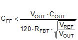
9.2.1.2.9 CFF Selection
In some cases, a feedforward capacitor can be used across RFBT to improve the load transient response or improve the loop-phase margin. This is especially true when values of RFBT > 100 kΩ are used. Large values of RFBT, in combination with the parasitic capacitance at the FB pin, can create a small signal pole that interferes with the loop stability. A CFF can help to mitigate this effect. Equation 9 can be used to estimate the value of CFF. The value found with Equation 9 is a starting point; use lower values to determine if any advantage is gained by the use of a CFF capacitor. The Optimizing Transient Response of Internally Compensated DC-DC Converters with Feed-forward Capacitor Application Report is helpful when experimenting with a feedforward capacitor.