JAJSFY3D August 2018 – August 2022 LMR36006-Q1
PRODUCTION DATA
- 1 特長
- 2 アプリケーション
- 3 概要
- 4 Revision History
- 5 Device Comparison Table
- 6 Pin Configuration and Functions
- 7 Specifications
- 8 Detailed Description
-
9 Application and Implementation
- 9.1 Application Information
- 9.2
Typical Application
- 9.2.1
Design 1: Low Power 24-V, 600-mA PFM Converter
- 9.2.1.1 Design Requirements
- 9.2.1.2
Detailed Design Procedure
- 9.2.1.2.1 Custom Design With WEBENCH Tools
- 9.2.1.2.2 Choosing the Switching Frequency
- 9.2.1.2.3 Setting the Output Voltage
- 9.2.1.2.4 Inductor Selection
- 9.2.1.2.5 Output Capacitor Selection
- 9.2.1.2.6 Input Capacitor Selection
- 9.2.1.2.7 CBOOT
- 9.2.1.2.8 VCC
- 9.2.1.2.9 CFF Selection
- 9.2.1.2.10 Maximum Ambient Temperature
- 9.2.1.3 Application Curves
- 9.2.2 Design 2: High Density 12-V , 600-mA FPWM Converter
- 9.2.1
Design 1: Low Power 24-V, 600-mA PFM Converter
- 9.3 What to Do and What Not to Do
- 10Power Supply Recommendations
- 11Layout
- 12Device and Documentation Support
- 13Mechanical, Packaging, and Orderable Information
パッケージ・オプション
メカニカル・データ(パッケージ|ピン)
- RNX|12
サーマルパッド・メカニカル・データ
- RNX|12
発注情報
9.2.1.2.5 Output Capacitor Selection
The value of the output capacitor and its ESR determine the output voltage ripple and load transient performance. The output capacitor bank is usually limited by the load transient requirements rather than the output voltage ripple. Equation 6 can be used to estimate a lower bound on the total output capacitance, and an upper bound on the ESR, required to meet a specified load transient.
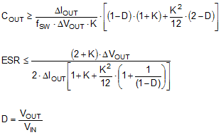
where
- ΔVOUT = output voltage transient
- ΔIOUT = output current transient
- K = ripple factor from Section 9.2.1.2.4
Once the output capacitor and ESR have been calculated, Equation 7 can be used to check the output voltage ripple.
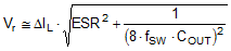
where
- Vr = peak-to-peak output voltage ripple
The output capacitor and ESR can then be adjusted to meet both the load transient and output ripple requirements.
In practice, the output capacitor has the most influence on the transient response and loop phase margin. Load transient testing and bode plots are the best way to validate any given design and must always be completed before the application goes into production. In addition to the required output capacitance, a small ceramic placed on the output can help reduce high frequency noise. Small case size ceramic capacitors in the range of 1 nF to 100 nF can be very helpful in reducing spikes on the output caused by inductor and board parasitics.
Limit the maximum value of total output capacitance to about 10 times the design value, or 1000 µF, whichever is smaller. Large values of output capacitance can adversely affect the start-up behavior of the regulator as well as the loop stability. If values larger than noted here must be used, then a careful study of start-up at full load and loop stability must be performed.