JAJSF63D April   2018  – September 2020 LMR36015

PRODUCTION DATA  

  1. 特長
  2. アプリケーション
  3. 概要
  4. Revision History
  5. 概要 (続き)
  6. Device Comparison Table
  7. Pin Configuration and Functions
    1.     Pin Functions
  8. Specifications
    1. 8.1 Absolute Maximum Ratings
    2. 8.2 ESD Ratings
    3. 8.3 Recommended Operating Conditions
    4. 8.4 Thermal Information
    5. 8.5 Electrical Characteristics
    6. 8.6 Timing Requirements
    7. 8.7 System Characteristics
    8. 8.8 Typical Characteristics
  9. Detailed Description
    1. 9.1 Overview
    2. 9.2 Functional Block Diagram
    3. 9.3 Feature Description
      1. 9.3.1 Power-Good Flag Output
      2. 9.3.2 Enable and Start-up
      3. 9.3.3 Current Limit and Short Circuit
      4. 9.3.4 Undervoltage Lockout and Thermal Shutdown
    4. 9.4 Device Functional Modes
      1. 9.4.1 Auto Mode
      2. 9.4.2 Forced PWM Operation
      3. 9.4.3 Dropout
      4. 9.4.4 Minimum Switch On-Time
  10. 10Application and Implementation
    1. 10.1 Application Information
    2. 10.2 Typical Application
      1. 10.2.1 Design 1: Low Power 24-V, 1.5-A PFM Converter
        1. 10.2.1.1 Design Requirements
        2. 10.2.1.2 Detailed Design Procedure
          1. 10.2.1.2.1  Custom Design With WEBENCH Tools
          2. 10.2.1.2.2  Choosing the Switching Frequency
          3. 10.2.1.2.3  Setting the Output Voltage
          4. 10.2.1.2.4  Inductor Selection
          5. 10.2.1.2.5  Output Capacitor Selection
          6. 10.2.1.2.6  Input Capacitor Selection
          7. 10.2.1.2.7  CBOOT
          8. 10.2.1.2.8  VCC
          9. 10.2.1.2.9  CFF Selection
            1. 10.2.1.2.9.1 External UVLO
          10. 10.2.1.2.10 Maximum Ambient Temperature
      2. 10.2.2 Application Curves
      3. 10.2.3 Design 2: High Density 24-V, 1.5-A FPWM Converter
        1. 10.2.3.1 Design Requirements
        2. 10.2.3.2 Detailed Design Procedure
        3. 10.2.3.3 Application Curves
    3. 10.3 What to Do and What Not to Do
  11. 11Power Supply Recommendations
  12. 12Layout
    1. 12.1 Layout Guidelines
      1. 12.1.1 Ground and Thermal Considerations
    2. 12.2 Layout Example
  13. 13Device and Documentation Support
    1. 13.1 Device Support
      1. 13.1.1 Development Support
        1. 13.1.1.1 Custom Design With WEBENCH® Tools
    2. 13.2 Documentation Support
      1. 13.2.1 Related Documentation
    3. 13.3 Receiving Notification of Documentation Updates
    4. 13.4 Support Resources
    5. 13.5 Trademarks
    6. 13.6 静電気放電に関する注意事項
    7. 13.7 Glossary
  14. 14Mechanical, Packaging, and Orderable Information

パッケージ・オプション

メカニカル・データ(パッケージ|ピン)
サーマルパッド・メカニカル・データ
発注情報

Application Curves

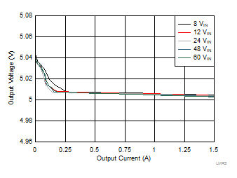
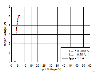
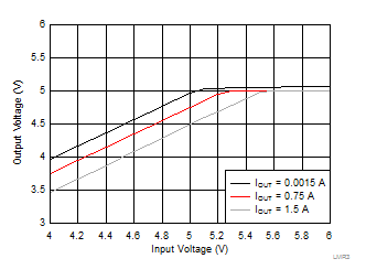
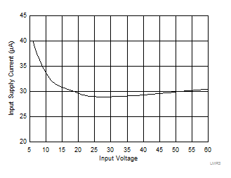
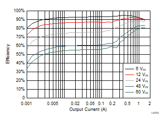
Unless otherwise specified the following conditions apply: VIN = 24 V, TA = 25°C. The circuit is shown in Figure 10-1, with the appropriate BOM from Table 10-3.
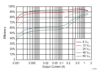
GUID-20200813-CA0I-QGQK-SNDH-TH0KS9JNZ270-low.gif
VOUT = 5 V 400 kHz
Figure 10-4 Efficiency
GUID-102AB987-3CA7-4299-ACB1-B70FE97F2E58-low.gif
VOUT = 5 V 400 kHz
Figure 10-6 Load Regulation
GUID-BC0F9857-5740-4D44-B655-6DB5222960B2-low.gif
VOUT = 5 V 400 kHz
Figure 10-8 Line Regulation
GUID-6E1A9327-0DA3-4E4C-A801-60328B1364AE-low.gif
VOUT = 5 V 400 kHz
Figure 10-10 Overall Dropout Characteristic
GUID-65E72FAF-4029-42D3-94AB-9DFC3C2901B4-low.gif
VOUT = 3.3 V IOUT= 0 A RFBT= 100 kΩ
Figure 10-12 Input Supply Current
GUID-12D5C160-063A-4089-9088-407628D4D895-low.jpg
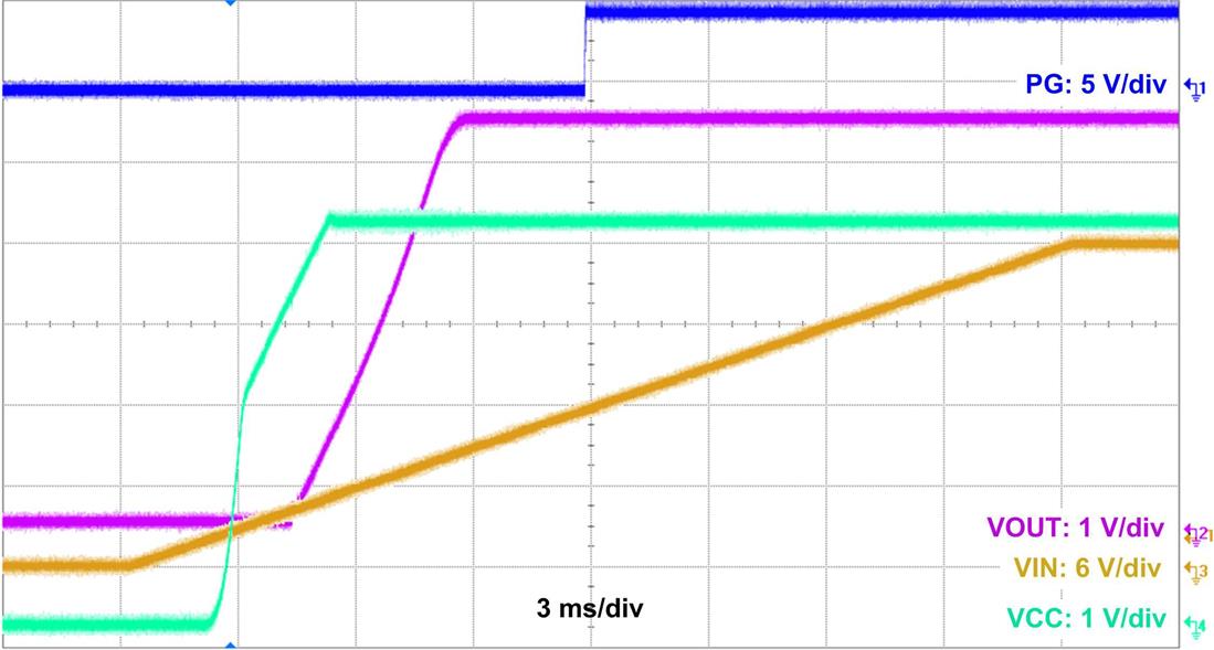
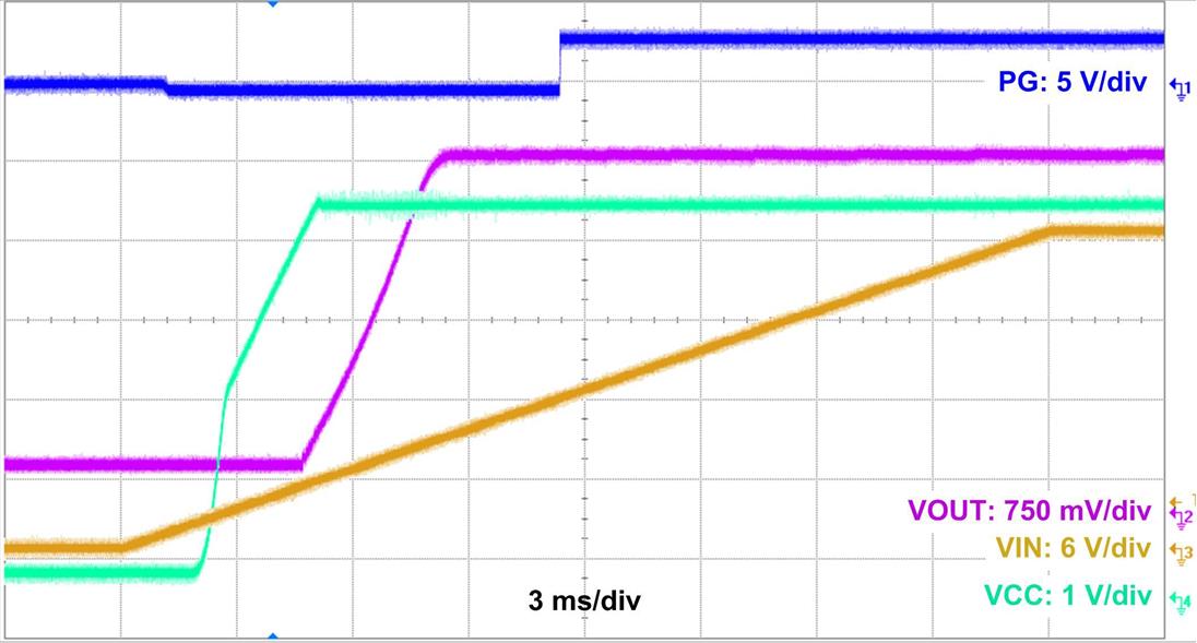
VOUT = 5 V 400 kHz
Figure 10-14 Start-Up Waveform
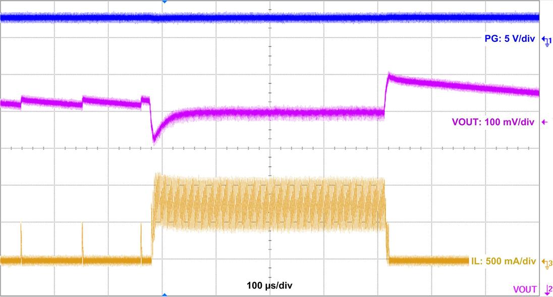
GUID-ACF902A5-A051-4902-A94F-7D57950C421C-low.jpg
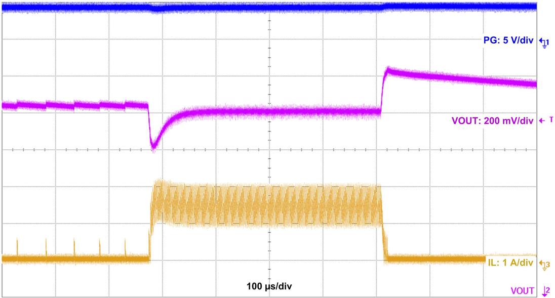
VOUT = 5 V 400 kHz
ILOAD= 10 mA - 0.75 A Slew Rate = 1 µs/A
Figure 10-16 Load Transient
GUID-BD5F896F-4000-4F67-92D0-D8E03932B8B1-low.gif
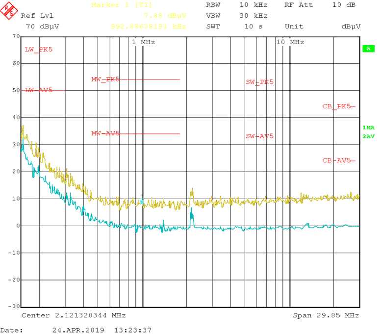
VIN = 13.5 V VOUT = 5 V IOUT = 1.5 A
Frequency Tested: 150 kHz to 30 MHz
Figure 10-18 Conducted EMI vs. CISPR25 Limits (Yellow: Peak Signal, Blue: Average Signal)
GUID-D281354C-75EE-4ACA-89ED-5C44F77ACCA9-low.gif
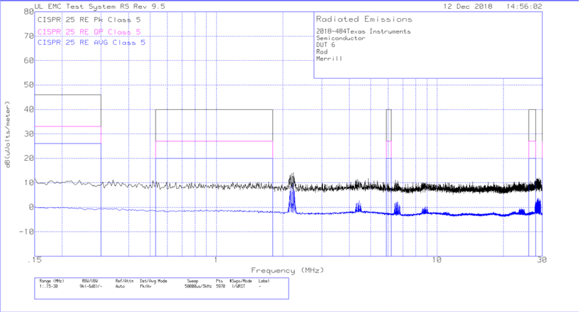
VIN = 13.5 V VOUT = 5 V IOUT = 1.5 A
Frequency Tested: 150 kHz to 30 MHz
Figure 10-20 Radiated EMI Rod vs. CISPR25 Limits
GUID-2670F2C6-1A86-4804-84EB-15CA1C2663B9-low.gif
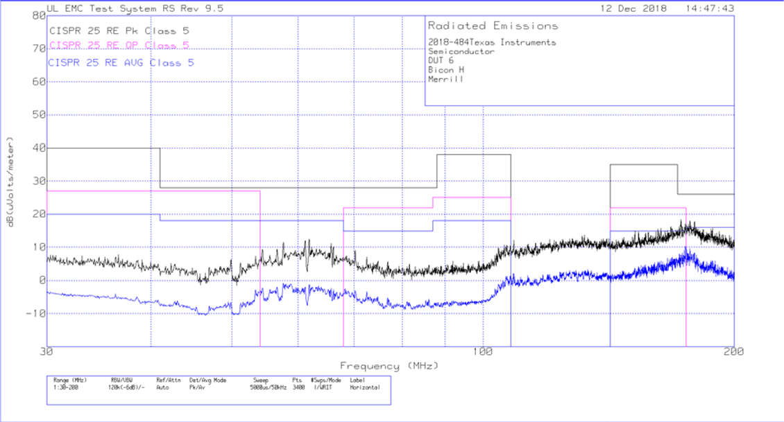
VIN = 13.5 V VOUT = 5 V IOUT = 1.5 A
Frequency Tested: 30 MHz to 200 MHz
Figure 10-22 Radiated EMI Bicon Horizontal vs. CISPR25 Limits
GUID-8418793B-ED8E-4212-99AB-788F264F9D73-low.gif
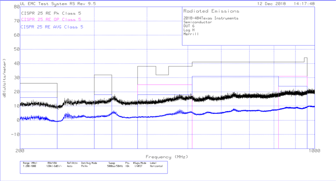
VIN = 13.5 V VOUT = 5 V IOUT = 1.5 A
Frequency Tested: 200 MHz to 1 GHz
Figure 10-24 Radiated EMI Log Horizontal vs. CISPR25 Limits
GUID-FDABBD51-BBAF-4AF2-9C00-162B3B7A2D3A-low.gif
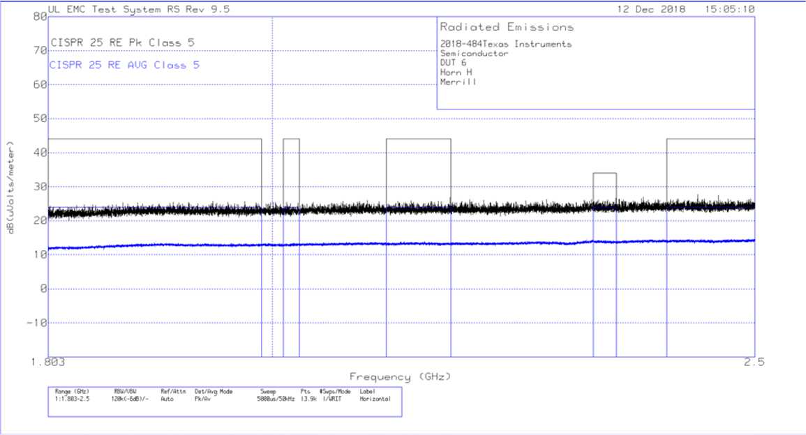
VIN = 13.5 V VOUT = 5 V IOUT = 1.5 A
Frequency Tested: 1.8 GHz to 2.5 GHz
Figure 10-26 Radiated EMI Horn Horizontal vs. CISPR25 Limits
GUID-8B88E362-D345-47E8-A309-E2F2FA91223A-low.gif
VOUT = 3.3 V 400 kHz
Figure 10-5 Efficiency
GUID-EFC8A410-D17F-4E0E-B7C7-E07BAA164511-low.gif
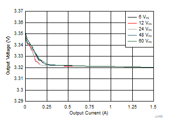
VOUT = 3.3 V 400 kHz
Figure 10-7 Load Regulation
GUID-9E102639-C335-49A5-B5FE-D91427CD850C-low.gif
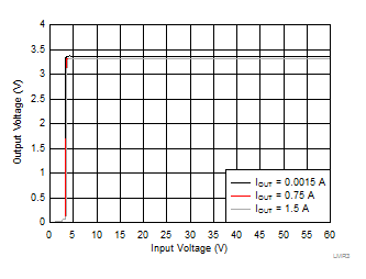
VOUT = 3.3 V 400 kHz
Figure 10-9 Line Regulation
GUID-2DC6D936-7DE3-4FC9-8375-371B00F71582-low.gif
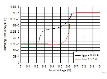
VOUT = 5 V 400 kHz
Figure 10-11 Frequency Dropout Characteristic
GUID-C35CF3A0-1A83-4EAD-9C01-00235975F472-low.gif
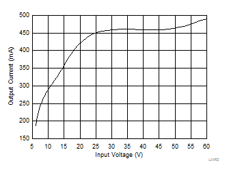
VOUT = 3.3 V 400 kHz
Figure 10-13 Mode Change Thresholds
GUID-54A66918-A200-4FCB-997C-A2DD1AD3B708-low.jpg
VOUT = 3.3 V 400 kHz
Figure 10-15 Start-Up Waveform
GUID-4F060841-9197-4285-8A73-77CEA76544EF-low.jpg
VOUT = 3.3 V 400 kHz
ILOAD= 10 mA - 0.75 A Slew Rate = 1 µs/A
Figure 10-17 Load Transient
GUID-E2B3B7CC-3F2B-4929-BEFB-B59FC878ACDA-low.gif
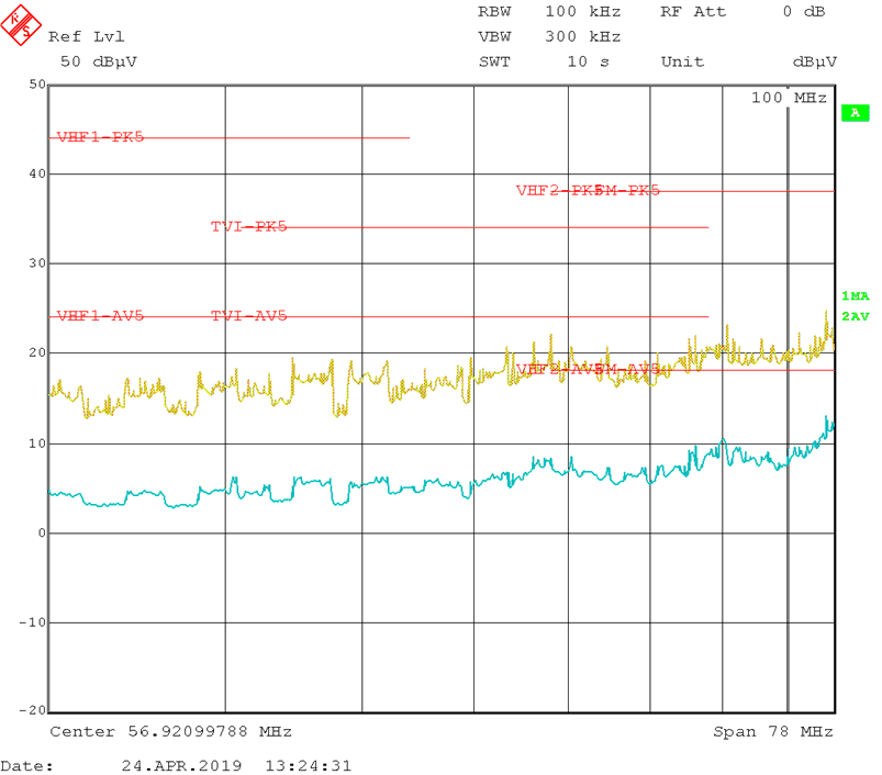
VIN = 13.5 V VOUT = 5 V IOUT = 1.5 A
Frequency Tested: 30 MHz to 108 MHz
Figure 10-19 Conducted EMI vs. CISPR25 Limits (Yellow: Peak Signal, Blue: Average Signal)
GUID-E07D1D9A-C3E3-4786-850A-F45087EF1730-low.gif
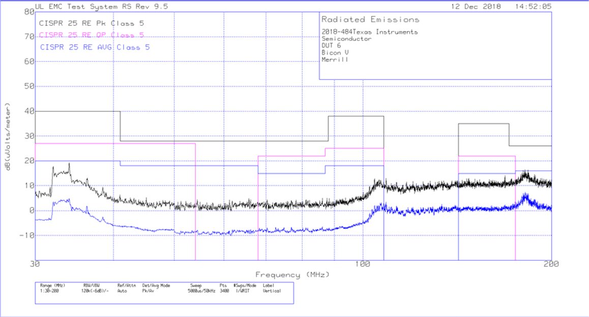
VIN = 13.5 V VOUT = 5 V IOUT = 1.5 A
Frequency Tested: 30 MHz to 200 MHz
Figure 10-21 Radiated EMI Bicon Vertical vs. CISPR25 Limits
GUID-8379BC52-2940-4599-B67A-C886F196674E-low.gif
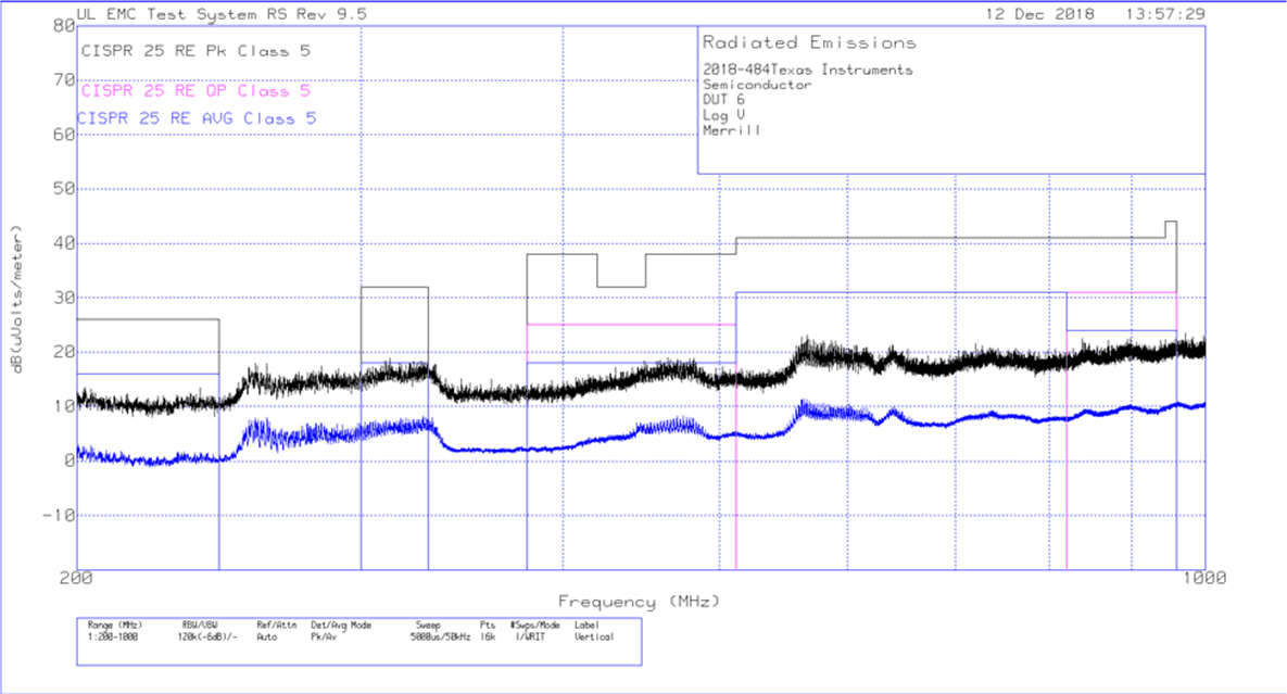
VIN = 13.5 V VOUT = 5 V IOUT = 1.5 A
Frequency Tested: 200 MHz to 1 GHz
Figure 10-23 Radiated EMI Log Vertical vs. CISPR25 Limits
GUID-983B9512-2159-4271-9687-0081095A113D-low.gif
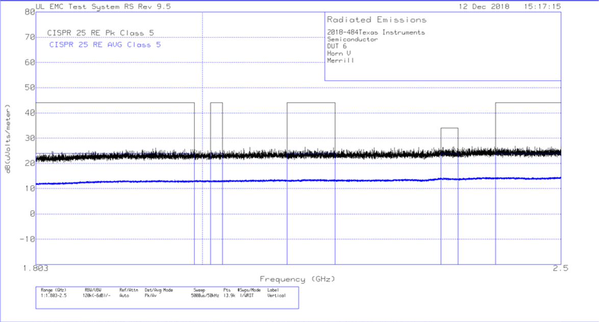
VIN = 13.5 V VOUT = 5 V IOUT = 1.5 A
Frequency Tested: 1.83 GHz to 2.5 GHz
Figure 10-25 Radiated EMI Horn Vertical vs. CISPR25 Limits
GUID-B826DA35-38CB-408D-AE77-F055BE732404-low.gif


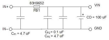
Figure 10-27 Recommended Input EMI Filter