JAJSDW2C November 2016 – August 2021 LMS3635-Q1 , LMS3655-Q1
PRODUCTION DATA
- 1 特長
- 2 アプリケーション
- 3 概要
- 4 Revision History
- 5 Device Comparison Tables
- 6 Pin Configuration and Functions
- 7 Specifications
- 8 Detailed Description
-
9 Application and Implementation
- 9.1 Application Information
- 9.2
Typical Applications
- 9.2.1
General Application
- 9.2.1.1 Design Requirements
- 9.2.1.2 Detailed Design Procedure
- 9.2.1.3 Application Curves
- 9.2.2 Fixed 5-V Output for USB-Type Applications
- 9.2.3 Fixed 3.3-V Output
- 9.2.4 6-V Adjustable Output
- 9.2.1
General Application
- 9.3 Do's and Don't's
- 10Power Supply Recommendations
- 11Layout
- 12Device and Documentation Support
- 13Mechanical, Packaging, and Orderable Information
パッケージ・オプション
メカニカル・データ(パッケージ|ピン)
- RNL|22
サーマルパッド・メカニカル・データ
- RNL|22
発注情報
8.3.4 Current Limit
The LMS36x5-Q1 incorporates a valley current limit for normal overloads and for short-circuit protection. A precision low-side current limit prevents excessive average output current from the buck converter of the LMS36x5-Q1. A high-side peak-current limit is employed for protection of the top N MOSFET and inductors. The two current limits enable use of smaller inductors than a system with a single current limit. This scheme allows use of inductors with saturation current rated less than twice the operating current of the LMS36x5-Q1.
During overloads the low-side current limit, IL-LS (see Section 7.6), determines the maximum load current that the LMS36x5-Q1 can supply. When the low-side switch turns on, the inductor current begins to ramp down. If the current does not fall below IL-LS before the next turnon cycle, then that cycle is skipped, and the low-side FET is left on until the current falls below IL-LS. This is different than the more typical peak current limit, and results in Equation 1 for the maximum load current.

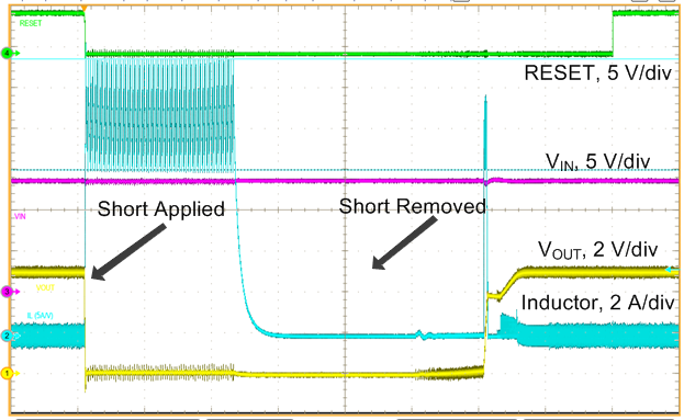
If the converter continues triggering valley current limit for more than about 64 clock cycles, the device turns off both high and low side switches for approximately 6 ms (see TW in Section 7.8). If the overload is still present after the hiccup time, another 64 cycles is counted, and the process is repeated. If the current limit is not tripped for two consecutive clock cycles, the counter is reset. The hiccup time allows the inductor current to fall to zero, resetting the inductor volt-second balance. Of course the output current is greatly reduced in this condition . A typical short-circuit transient and recovery is shown in Figure 8-5.
 Figure 8-5 Short-Circuit Transient and Recovery
The high-side current limit trips when the peak inductor current reaches IL-HS (see Section 7.6). This is a cycle-by-cycle current limit and does not produce any frequency or current foldback. It is meant to protect the high-side MOSFET from excessive current. Under some conditions, such as high input voltage, this current limit may trip before the low-side protection. The peak value of this current limit varies with duty cycle.
In response to a short circuit, the peak current limit prevents excessive peak current while valley current limit prevents excessive average inductor current and keeps the power dissipation low during a fault. After a small number of cycles of valley current limit triggers, hiccup mode is activated.
In addition, the INEG current limit also protects the low-side switch from excessive negative current when the device is in FPWM mode. If this current exceeds INEG, the low-side switch is turned off until the next clock cycle. When the device is in AUTO mode, the negative current limit is increased to about IZC (about 0 A). This allows the device to operate in DCM.